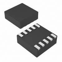
MAX4745ELB+T Maxim Integrated Products, MAX4745ELB+T Datasheet - Page 9

MAX4745ELB+T
Manufacturer Part Number
MAX4745ELB+T
Description
IC SWITCH DUAL SPDT 10UDFN
Manufacturer
Maxim Integrated Products
Datasheet
1.MAX4744ELBT.pdf
(12 pages)
Specifications of MAX4745ELB+T
Function
Audio Switch
Circuit
2 x SPDT
On-state Resistance
950 mOhm
Voltage Supply Source
Single Supply
Voltage - Supply, Single/dual (±)
1.8 V ~ 5.5 V
Current - Supply
0.3µA
Operating Temperature
-40°C ~ 85°C
Mounting Type
Surface Mount
Package / Case
10-µDFN
Lead Free Status / RoHS Status
Lead free / RoHS Compliant
Other names
MAX4745ELB+T
MAX4745ELB+TTR
MAX4745ELB+TTR
Figure 2. Switching Time
Figure 3. Break-Before-Make Interval
step DC voltage is switched into the speaker. The DC
step transients can be reduced by automatically dis-
charging the side that is not connected to the COM ter-
minal, reducing any residual DC voltage and reducing
clicks and pops.
All devices feature break-before-make switching which
is configured to break (open) the first set of contacts
before engaging (closing) the new contacts. This pre-
vents the momentary connection of the old and new sig-
nal paths to the output, reducing click-and-pop sounds.
MAX4744H/MAX4745H
MAX4744H/MAX4745H
MAX4744/MAX4745/
MAX4744/MAX4745/
V
NC_
LOGIC
INPUT
V
= V
LOGIC
INPUT
NC_
NO_
OR V
Break-Before-Make Switching
Low-Voltage, Dual SPDT, Audio Clickless
_______________________________________________________________________________________
NO_
Switches With Negative Rail Capability
C
V
C
L
OUT
L
NC_
NO_
CB_
INCLUDES FIXTURE AND STRAY CAPACITANCE
NO_
OR NC_
INCLUDES FIXTURE AND STRAY CAPACITANCE
CB_
= V
GND
N_
(
R
L
GND
R
+ R
L
ON
V
V
)
CC
CC
V
V
COM_
COM_
CC
CC
R
R
L
L
V
OUT
C
C
L
L
V
OUT
Caution: Do not exceed the Absolute Maximum
Ratings since stresses beyond the listed ratings
may cause permanent damage to the device.
Proper power-supply sequencing is recommended for
all CMOS devices. Improper supply sequencing can
force the switch into latch-up causing it to draw exces-
sive supply current. The only way out of latch-up is to
recycle the power and reapply properly. Connect all
ground pins first, then apply power to V
apply signals to NO_, NC_, and COM_. Follow the
reverse order upon power-down.
SWITCH
OUTPUT
LOGIC
INPUT
Test Circuits/Timing Diagrams
LOGIC
INPUT
V
OUT
V
0V
0V
CC
V
CC
0V
Power-Supply Sequencing and
IN DEPENDS ON SWITCH CONFIGURATION;
INPUT POLARITY DETERMINED BY SENSE OF SWITCH.
V
t
50%
50%
ON
OUT
Overvoltage Protection
0.8 x V
t
BBM
0UT
t
OFF
0.9 x V
t r < 5ns
t f < 5ns
0.2 x V
CC
OUT
, and finally
OUT
9


