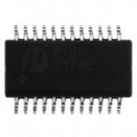
PI3V512QE Pericom Semiconductor, PI3V512QE Datasheet - Page 3

PI3V512QE
Manufacturer Part Number
PI3V512QE
Description
IC 2:1 MUX/DEMUX SW 5PORT 24QSOP
Manufacturer
Pericom Semiconductor
Datasheet
1.PI3V512QE.pdf
(8 pages)
Specifications of PI3V512QE
Function
Video Multiplexer/Demultiplexer
Circuit
5 x 2:1
On-state Resistance
8 Ohm
Voltage Supply Source
Single Supply
Voltage - Supply, Single/dual (±)
3 V ~ 3.6 V
Current - Supply
800µA
Operating Temperature
-40°C ~ 85°C
Mounting Type
Surface Mount
Package / Case
24-QSOP
Number Of Channels
5 Channel
On Resistance (max)
8 Ohms @ 3.3 V @ - 40 C to 85 C
Propagation Delay Time
0.25 ns (Typ)
On Time (max)
15 ns
Off Time (max)
9 ns
Supply Voltage (max)
3.6 V
Supply Voltage (min)
3 V
Maximum Power Dissipation
500 mW
Maximum Operating Temperature
+ 85 C
Minimum Operating Temperature
- 40 C
Mounting Style
SMD/SMT
Lead Free Status / RoHS Status
Lead free / RoHS Compliant
Available stocks
Company
Part Number
Manufacturer
Quantity
Price
Company:
Part Number:
PI3V512QE
Manufacturer:
PERICOM
Quantity:
25
Part Number:
PI3V512QE
Manufacturer:
PERICOM
Quantity:
20 000
Company:
Part Number:
PI3V512QEX
Manufacturer:
TOSHIBA
Quantity:
40 492
Part Number:
PI3V512QEX
Manufacturer:
PERICOM
Quantity:
20 000
DC Electrical Characteristics
Capacitance
Notes:
1. For max. or min. conditions, use appropriate value specified under Electrical Characteristics for the applicable device type.
2. Typical values are at V
3. Measured by the voltage drop between Y and I pins at indicated current through the switch. On-Resistance is determined by the lower of the
4. This parameter is determined by device characterization but is not production tested.
Power Supply Characteristics
Notes:
1. For max. or min. conditions, use appropriate value specified under Electrical Characteristics for the applicable device type.
2. Typical values are at V
3. Per TTL driven input (control inputs only); Y and I pins do not contribute to I
V
V
V
I
I
I
R
R
∆R
C
C
C
I
Paramenter
Parameters
Parameters
IH
IL
OFF
CC
voltages on the two (Y & I) pins.
ON
FLAT(ON)
IN
OFF(IN0, IN1)
ON(Y/I)
IH
IL
IK
ON
10-0250
(5)
Input HIGH Voltage
Input LOW Voltage
Clamp Diode Voltage
Input HIGH Current
Input LOW Current
Power Down Leakage Current
Switch On-Resistance
On-Resistance Flatness
On-Resistance match from center
ports to any other port
Description
(T A = 25°C, f = 1MHz)
Quiescent Power Supply Current
Description
DD
DD
Input Capacitance
Port I Capacitance, Switch OFF
Y/I Capacitance, Switch ON
Description
= 3.3V, T
= 3.3V, T
A
A
= 25°C ambient and maximum loading.
= 25°C ambient and maximum loading.
(3)
(4)
(4)
(T A = –40°C to +85°C, V DD = 3.3V ±10%)
V
DD
Guaranteed HIGH level
Guaranteed LOW level
V
V
V
V
V
I
V
I
V
I
Test Conditions
IN
IN
IN
DD
DD
DD
DD
DD
DD
DD
= Max., V
= –10mA to –30mA
= –10mA to –30mA
= –10mA to –30mA
Test Conditions
= Max., V
= Max., I
= Max., V
= 0V, V
= Min., 1.25V ≤ V
= Min., V
= Min., 1.25V ≤ V
3
Low On-Resistance, 3.3V Wideband/Video Switch
A
IN
= 0V, V
V
IN
Test Conditions
CC
IN
IN
IN
= GND or V
IN
.
= –18mA
@ 1.25V and V
= V
= GND
= 0V
DD
B
(1)
IN
≤ 3.6
IN
≤ V
≤ V
DD
DD,
DD,
DD,
-
Min.
2.0
4.0
6.0
Typ.
2.0
–0.5
-
-
-
-
-
-
-
Min. Typ.
5-Port 2:1 Mux/DeMux
-
Typ.
-
-
–0.7
-
-
-
-
1.0
0.9
3.0
6.0
10.0
Max.
(2)
(2)
PS8752C
800
Max.
-
0.8
–1.2
±5
±5
-
8
-
2.0
Max.
PI3V512
pF
Units
V
µA
Ω
Units
µA
Units
02/16/11


