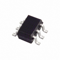
ADG749BKSZ-REEL7 Analog Devices Inc, ADG749BKSZ-REEL7 Datasheet - Page 11

ADG749BKSZ-REEL7
Manufacturer Part Number
ADG749BKSZ-REEL7
Description
IC SWITCH SPDT SC70-6
Manufacturer
Analog Devices Inc
Type
Analog Switchr
Datasheet
1.ADG749BKSZ-REEL.pdf
(12 pages)
Specifications of ADG749BKSZ-REEL7
Function
Switch
Circuit
1 x SPDT
On-state Resistance
5 Ohm
Voltage Supply Source
Single Supply
Voltage - Supply, Single/dual (±)
1.8 V ~ 5.5 V
Current - Supply
0.001µA
Operating Temperature
-40°C ~ 85°C
Mounting Type
Surface Mount
Package / Case
6-TSSOP, SC-88, SOT-363
Analog Switch Type
SPDT
No. Of Channels
1
Bandwidth
200MHz
On State Resistance Max
2.5ohm
Turn Off Time
3ns
Turn On Time
7ns
Supply Voltage Range
1.8V To 5.5V
Multiplexer Configuration
Single SPDT
Number Of Inputs
1
Number Of Outputs
2
Number Of Channels
1
Analog Switch On Resistance
12@3VOhm
Analog Switch Turn On Time
10ns
Analog Switch Turn Off Time
4ns
Package Type
SC-70
Power Supply Requirement
Single
Single Supply Voltage (min)
1.8V
Single Supply Voltage (typ)
3/5V
Single Supply Voltage (max)
5.5V
Dual Supply Voltage (min)
Not RequiredV
Dual Supply Voltage (typ)
Not RequiredV
Dual Supply Voltage (max)
Not RequiredV
Power Dissipation
315mW
Supply Current
0.001mA
Mounting
Surface Mount
Pin Count
6
Operating Temp Range
-40C to 125C
Operating Temperature Classification
Automotive
Lead Free Status / RoHS Status
Lead free / RoHS Compliant
Lead Free Status / RoHS Status
Lead free / RoHS Compliant, Lead free / RoHS Compliant
Other names
ADG749BKSZ-REEL7TR
Available stocks
Company
Part Number
Manufacturer
Quantity
Price
Company:
Part Number:
ADG749BKSZ-REEL7
Manufacturer:
AD
Quantity:
500
Company:
Part Number:
ADG749BKSZ-REEL7
Manufacturer:
NSC
Quantity:
147
Part Number:
ADG749BKSZ-REEL7
Manufacturer:
ADI/亚德诺
Quantity:
20 000
APPLICATIONS INFORMATION
The ADG749 belongs to Analog Devices’ new family of CMOS
switches. This series of general-purpose switches has improved
switching times, offering lower on resistance, higher band-
widths, low power consumption, and low leakage currents.
ADG749 SUPPLY VOLTAGES
Functionality of the ADG749 extends from 1.8 V to 5.5 V single
supply, which makes it ideal for battery-powered instruments,
where power efficiency and performance are important design
parameters.
It is important to note that the supply voltage affects the input
signal range, the on resistance, and the switching times of the
part. By taking a look at the typical performance characteristics
and the specifications, the effects of the power supplies can be
clearly seen.
For V
temperature range.
ON RESPONSE VS. FREQUENCY
Figure 21 illustrates the parasitic components that affect the
ac performance of CMOS switches (the switch is shown
surrounded by a box). Additional external capacitances will
further degrade some performance. These capacitances affect
feedthrough, crosstalk, and system bandwidth.
The transfer function that describes the equivalent diagram of
the switch (Figure 21) is of the form A(s) shown below.
where:
The signal transfer characteristic is dependent on the switch
channel capacitance, C
zero in the numerator of the transfer function A(s). Because the
Figure 21. Switch Represented by Equivalent Parasitic Components
R
C
A
DD
T
T
(
s
= R
= C
= 1.8 V operation, R
)
=
V
S
LOAD
IN
LOAD
R
T
⎡
⎢
⎢ ⎣
/(R
+ C
s
(
s
R
LOAD
(
T
D
R
R
C
ON
+ C
R
ON
DS
+ R
DS
ON
C
. This capacitance creates a frequency
DS
DS
C
ON
C
D
DS
)
)
ON
+
)
+ 1
1
is typically 40 Ω over the
⎤
⎥
⎥ ⎦
C
LOAD
D
R
LOAD
V
OUT
Rev. B | Page 11 of 12
switch on resistance is small, this zero usually occurs at high
frequencies. The bandwidth is a function of the switch output
capacitance combined with C
frequency pole corresponding to these capacitances appears in
the denominator of A(s).
The dominant effect of the output capacitance, C
pole breakpoint frequency to occur first. Therefore, in order
to maximize bandwidth, a switch must have a low input and
output capacitance and low on resistance. The on response vs.
frequency plot for the ADG749 is shown in Figure 11.
OFF ISOLATION
Off isolation is a measure of the input signal coupled through
an off switch to the switch output. The capacitance, C
the input signal to the output load when the switch is off, as
shown in Figure 22.
The larger the value of CDS, the larger the values of feed-
through that will be produced. The typical performance
characteristic graph of Figure 9 illustrates the drop in off
isolation as a function of frequency. From dc to roughly
200 kHz, the switch shows better than −95 dB isolation. Up to
frequencies of 10 MHz, the off isolation remains better than
−67 dB. As the frequency increases, more and more of the input
signal is coupled through to the output. Off isolation can be
maximized by choosing a switch with the smallest C
The values of load resistance and capacitance also affect off
isolation, since they contribute to the coefficients of the poles
and zeros in the transfer function of the switch when open.
A
Figure 22. Off Isolation is Affected by External Load Resistance
(
s
)
=
V
S
IN
⎡
⎢
⎢
⎣
s
(
R
LOAD
C
)
DS
(
s
C
(
R
and Capacitance
LOAD
LOAD
C
D
DS
+
C
and the load capacitance. The
C
DS
D
C
)
+
LOAD
D
C
DS
)
+
R
1
LOAD
⎤
⎥
⎥
⎦
D
, causes the
ADG749
DS
V
DS
OUT
possible.
, couples


