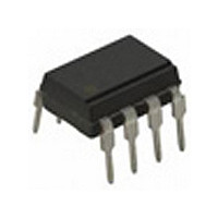
AD743JN Analog Devices Inc, AD743JN Datasheet - Page 11

AD743JN
Manufacturer Part Number
AD743JN
Description
Manufacturer
Analog Devices Inc
Type
General Purpose Amplifierr
Datasheet
1.AD743JN.pdf
(12 pages)
Specifications of AD743JN
Rail/rail I/o Type
No
Number Of Elements
1
Unity Gain Bandwidth Product
4.5MHz
Slew Rate
2.8V/us
Common Mode Rejection Ratio
80dB
Input Offset Voltage
1mV
Input Bias Current
200pA
Single Supply Voltage (typ)
Not RequiredV
Dual Supply Voltage (typ)
±15V
Voltage Gain In Db
132.04dB
Power Supply Rejection Ratio
90dB
Power Supply Requirement
Dual
Shut Down Feature
No
Single Supply Voltage (min)
Not RequiredV
Single Supply Voltage (max)
Not RequiredV
Dual Supply Voltage (min)
±4.8V
Dual Supply Voltage (max)
±18V
Technology
BiFET
Operating Temp Range
0C to 70C
Operating Temperature Classification
Commercial
Mounting
Through Hole
Pin Count
8
Package Type
PDIP
Lead Free Status / Rohs Status
Not Compliant
Available stocks
Company
Part Number
Manufacturer
Quantity
Price
REV. E
Figure 15b. AC-Coupled, Low Noise
Hydrophone Amplifier
Figure 15c. Hydrophone Amplifier Incorporating a
DC Servo Loop
HYDROPHONE
B AND K TYPE 8100
TYPE 8100
B AND K
HYDROPHONE
100
*OPTIONAL, SEE TEXT
**1V PER MICROPASCAL
INPUT SENSITIVITY = –179 dB re. 1V/ Pa**
R3
C
T
100
C
C
R3
10
T
C
DC OUTPUT
*OPTIONAL, SEE TEXT
R4*
8
10
1M
R2
Figure 17. Optional External Components for Balancing Source Impedances
8
R6
R1
R4*
10
R1
8
100k
C
C1*
S
R5
AD743
1mV FOR I
R
C
C1*
1900
B
B
AD743
R2
1900
R2
R
S
R
B
S
AD711K
(AD743)
0.27 F
>> R1 OR R2
C
R
NONINVERTING
CONNECTION
16M
C2
B
B
FOR
R7
A
A
R1
= C
= R
OUTPUT
S
S
OUTPUT
100nA
16M
OUTPUT
–11–
R
S
where the dc gain is 1 and the gain above the low frequency cutoff
(1/(2πC
circuit of Figure 15c uses a dc servo loop to keep the dc output
at 0 V and to maintain full dynamic range for I
The time constant of R7 and C2 should be larger than that of
R1 and C
The transducer shown has a source capacitance of 7500 pF. For
smaller transducer capacitances (≤300 pF), the lowest noise can
be achieved by adding a parallel RC network (R4 = R1, C1 = C
in series with the inverting input of the AD743.
BALANCING SOURCE IMPEDANCES
As mentioned previously, it is good practice to balance the
source impedances (both resistive and reactive) as seen by the
inputs of the AD743. Balancing the resistive components will
optimize dc performance over temperature because balancing
will mitigate the effects of any bias current errors. Balancing
input capacitance will minimize ac response errors due to the
amplifier’s input capacitance and, as shown in Figure 16, noise
performance will be optimized. Figure 17 shows the required
external components for noninverting (A) and inverting (B)
configurations.
C
S
Figure 16. RTI Voltage Noise vs. Input Capacitance
C
40
30
20
10
C
(100 Ω))) is the same as the circuit of Figure 15a. The
T
B
10
for a smooth low frequency response.
BALANCED
2.9nV/√Hz
R
B
C
F
R
C
B
B
B
R1
INVERTING
CONNECTION
= R1 R
= C
INPUT CAPACITORS (pF)
B
F
C
S
S
UNBALANCED
100
OUTPUT
B
up to 100 nA.
AD743
1000
T
)


