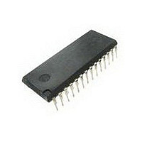
DG538ADJ Vishay, DG538ADJ Datasheet - Page 14

DG538ADJ
Manufacturer Part Number
DG538ADJ
Description
Analog Multiplexer Single 8:1 28-Pin PDIP
Manufacturer
Vishay
Type
Analog Multiplexerr
Specifications of DG538ADJ
Multiplexer Configuration
Single 8:1
Number Of Inputs
8
Number Of Outputs
2
Number Of Channels
1
Package Type
PDIP
Power Supply Requirement
Single/Dual
Single Supply Voltage (min)
10V
Single Supply Voltage (typ)
12/15V
Single Supply Voltage (max)
18V
Dual Supply Voltage (min)
±10V
Dual Supply Voltage (typ)
±12V
Dual Supply Voltage (max)
±15V
Power Dissipation
625mW
Mounting
Through Hole
Pin Count
28
Operating Temp Range
-40C to 85C
Operating Temperature Classification
Industrial
Package
28PDIP
Maximum On Resistance
90@15V@-3V Ohm
Maximum Propagation Delay Bus To Bus
300@15V|300@-3V ns
Maximum High Level Output Current
40 mA
Multiplexer Architecture
8:1
Number Of Channels Per Chip
1
Maximum Turn-off Time
175@15V@-3V ns
Maximum Turn-on Time
300@15V@-3V ns
Power Supply Type
Single|Dual
Lead Free Status / Rohs Status
Not Compliant
Available stocks
Company
Part Number
Manufacturer
Quantity
Price
Part Number:
DG538ADJ
Manufacturer:
INTERSIL
Quantity:
20 000
Device Description
The DG534A/538A D/CMOS wideband multiplexers offer
single-ended or differential functions. A 8/4 or 4/2 logic input
pin selects the single-ended or differential mode.
To meet the high dynamic performance demands of video,
high definition TV, digital data routing (in excess of 100 Mbps),
etc., the DG534A/538A are fabricated with DMOS transistors
configured in ‘T’ arrangements with second level ‘L’
configurations (see Functional Block Diagram).
Use of DMOS technology yields devices with very low
capacitance and low r
high frequency signal handling and higher switching speeds,
while maintaining low insertion loss figures. The ‘T’ and ‘L’
switch configurations further improve dynamic performance
by greatly reducing crosstalk and output node capacitances.
www.vishay.com
14
DG534A/538A
Vishay Siliconix
Symbol
A
0
, A
GND
S
S
S
S
WR
S
S
S
S
4/2
8/4
RS
EN
D
V+
I/O
V–
D
V
A1
A2
A3
A4
B4
B3
B2
B1
A
B
1
L
, A
2
DG534ADJ
DS(on)
11, 10, –
1, 5, 16
12
13
14
15
17
18
19
2
3
4
6
–
–
7
–
8
9
–
–
. This directly relates to improved
Pin Number
1, 5, 7, 9, 21, 23, 25
DG538A
16, 15, 14
10
11
12
13
17
18
19
20
22
24
26
27
28
2
3
4
6
8
–
Analog Output/Input
Positive Supply Voltage
Analog Input/Output
Analog Input/Output
Analog Input/Output
Analog Input/Output
4 x 1 or 2 x 2 Select
8 x 1 or 4 x 2 Select
Reset
Write command that latches A, EN
Binary address inputs that determine which channel(s) is/are connected to the out-
put(s)
Enable. Input/Output, if EN = 0, all channels are open
Input/Output control. Used to write to or read from the address latches
Logic Supply Voltage, usually +5 V
Analog Input/Output
Analog Input/Output
Analog Input/Output
Analog Input/Output
Negative Supply Voltage
Analog Output/Input
Analog and Digital Grounds. All grounds should be connected externally to optimize
dynamic performance
The
replacements for the non-A versions. Improvements include:
higher current readback drivers, readback of the EN bit,
latchup protection
Frequency Response
A single multiplexer on-channel exhibits both resistance
[r
causes a frequency dependent attenuation of the analog
signal. The –3-dB bandwidth of the DG534A/538A is typically
500 MHz (into 50 W). This figure of 500 MHz illustrates that the
switch-channel cannot be represented by a simple RC
combination. The on capacitance of the channel is distributed
along the on-resistance, and hence becomes a more complex
multi-stage network of R’s and C’s making up the total r
and C
DS(on)
S(on)
DG534A/DG538A
] and capacitance [C
.
Description
are
S(on)
improved
].
S-05734—Rev. G, 29-Jan-02
This RC combination
Document Number: 70069
pin-compatible
DS(on)


