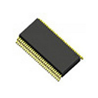
IDT74FST163232PA IDT, Integrated Device Technology Inc, IDT74FST163232PA Datasheet - Page 4

IDT74FST163232PA
Manufacturer Part Number
IDT74FST163232PA
Description
Manufacturer
IDT, Integrated Device Technology Inc
Datasheet
1.IDT74FST163232PA.pdf
(7 pages)
Specifications of IDT74FST163232PA
Configuration
16 x 2:1
Number Of Inputs
32
Number Of Outputs
16
Operating Supply Voltage (typ)
5V
Operating Supply Voltage (min)
4.5V
Operating Supply Voltage (max)
5.5V
Operating Temp Range
-40C to 85C
Operating Temperature Classification
Industrial
Mounting
Surface Mount
Pin Count
56
Package Type
TSSOP
Lead Free Status / Rohs Status
Not Compliant
Available stocks
Company
Part Number
Manufacturer
Quantity
Price
Company:
Part Number:
IDT74FST163232PA
Manufacturer:
IDT
Quantity:
6 219
NOTES:
1. For conditions shown as Max. or Min., use appropriate value specified under Electrical Characteristics for the applicable device type. T
2. Typical values are at V
3. Per TTL driven input (V
4. This parameter represents the current required to switch the internal capacitance of the control inputs at the specified frequency.
5. C
6. I
POWER SUPPLY CHARACTERISTICS
IDT74FST163232
16-BIT SYNCHRONOUS 2:1 MUX/DEMUX SWITCH
Symbol
Switch inputs generate no significant power supply currents as they transition. This parameter is not directly testable, but is derived for use in Total Power Supply Calculations.
C
I
I
ΔI
D
N
I
f
N = Number of Control Inputs Toggling at f
C
C
CC
CCD
i
PD
PD
H
T
= Control Input Frequency
ΔI
I
I
CC
= I
= I
CCD
CCD
I
= Number of TTL Inputs at D
= Duty Cycle for TTL Inputs High
= Quiescent Current
C
CC
= I
= Power Dissipation Capacitance
QUIESCENT
CC
= Dynamic Current Caused by an Input Transition Pair (HLH or LHL)
= Power Supply Current for a TTL High Input (V
CCD
+ ΔI
/V
CC
CC
Quiescent Power Supply Current
TTL Inputs HIGH
Dynamic Power Supply
Current
Dynamic Power Supply
Current
Total Power Supply Current
+ I
D
H
INPUTS
N
T
+ I
(4,5)
(4,5)
CC
+ I
CCD
IN
= 3.4V). All other inputs at V
DYNAMIC
= 5.0V, +25°C ambient.
Parameter
(f
i
N)
H
i
(6)
IN
CC
= 3.4V)
V
V
V
Clock Pin Toggling
50% Duty Cycle
16 Switches Toggling
One Select Toggling at
50% of CLK Frequency
V
Clock Pin Toggling
50% Duty Cycle
32 Switches Toggling
Two Select Pins Toggling at
50% of CLK Frequency
V
f
50% Duty Cycle
CLKEN = LOW
S
f
16 Switches Toggling
V
f
50% Duty Cycle
CLKEN = LOW
S
f
16 MUXes Exchanging
V
f
50% Duty Cycle
CLKEN = LOW
S
f
32 Switches Toggling
or GND. Switch inputs do not contribute to ΔI
CP
i
CP
i
CP
i
IN
CC
CC
CC
CC
0
CC
1
CC
1
= 2.5MHz (S
= 2.5MHz (S
= 2.5MHz (S
= LOW
= HIGH or LOW
= HIGH
= 3.4V
= 10MHz (CLK)
= 10MHz (CLK)
= 10MHz (CLK)
= Max.
= Max.
= Max.
= Max.
= Max.
= Max.
(3)
1
0
0
)
)
)
Test Conditions
4
V
V
V
V
V
V
V
V
V
V
V
V
V
V
V
V
(1)
IN
IN
IN
IN
IN
IN
IN
IN
IN
IN
IN
IN
IN
IN
IN
IN
= V
= V
= V
= V
= V
= V
= V
= V
= 3.4V
= 3.4V
= 3.4V
= GND
= GND
= GND
= GND
= GND
CC
CC
CC
CC
CC
CC
CC
CC
CC.
INDUSTRIAL TEMPERATURE RANGE
Min.
—
A
Typ.
= –40°C to +85°C
0.5
(2)
Max.
1.5
MHz/
MHz/
Unit
µA/
µA/
mA
mA


