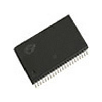
CY7C1049CV33-12ZI Cypress Semiconductor Corp, CY7C1049CV33-12ZI Datasheet - Page 5

CY7C1049CV33-12ZI
Manufacturer Part Number
CY7C1049CV33-12ZI
Description
Manufacturer
Cypress Semiconductor Corp
Datasheet
1.CY7C1049CV33-12ZI.pdf
(12 pages)
Specifications of CY7C1049CV33-12ZI
Density
4Mb
Access Time (max)
12ns
Sync/async
Asynchronous
Architecture
Not Required
Clock Freq (max)
Not RequiredMHz
Operating Supply Voltage (typ)
3.3V
Address Bus
19b
Package Type
TSOP-II
Operating Temp Range
-40C to 85C
Number Of Ports
1
Supply Current
95mA
Operating Supply Voltage (min)
3V
Operating Supply Voltage (max)
3.6V
Operating Temperature Classification
Industrial
Mounting
Surface Mount
Pin Count
44
Word Size
8b
Number Of Words
512K
Lead Free Status / Rohs Status
Not Compliant
Maximum Ratings
Exceeding maximum ratings may impair the useful life of the
device. These user guidelines are not tested.
Storage Temperature ................................. –65C to +150C
Ambient Temperature with
Power Applied ............................................ –55C to +125C
Supply Voltage on V
Voltage Applied to Outputs
in High-Z State
Electrical Characteristics
Over the Operating Range
Capacitance
Tested initially and after any design or process changes that may affect these parameters.
Thermal Resistance
Tested initially and after any design or process changes that may affect these parameters.
Notes
Document #: 38-05006 Rev. *H
V
V
V
V
I
I
I
I
C
C
2. V
3. Tested initially and after any design or process changes that may affect these parameters.
IX
CC
SB1
SB2
Parameter
OH
OL
IH
IL
IN
OUT
Parameter
IL
(min) = –2.0V and V
Parameter
JC
JA
Output HIGH Voltage
Output LOW Voltage
Input HIGH Voltage
Input LOW Voltage
Input Load Current
V
Supply Current
Automatic CE
Power Down Current
—TTL Inputs
Automatic CE
Power Down Current
—CMOS Inputs
[2]
CC
Thermal Resistance (Junction
to Ambient)
Thermal Resistance
(Junction to Case)
.................................... –0.5V to V
Operating
Description
CC
IH
(max) = V
to Relative GND
Input Capacitance
I/O Capacitance
Description
CC
+ 0.5V for pulse durations of less than 20 ns.
[2]
Description
V
V
GND < V
V
f = f
Max. V
V
V
Max. V
CE > V
V
or V
[2]
CC
CC
CC
IN
IN
IN
–0.5V to +4.6VDC
MAX
> V
< V
> V
IN
= Min.; I
= Min.,; I
= Max.,
< 0.3V, f = 0
CC
CC
CC
IH
IL
CC
= 1/t
, f = f
Test conditions follow standard
test methods and procedures for
measuring thermal impedance,
per EIA / JESD51.
I
, CE > V
,
or
< V
– 0.3V,
– 0.3V,
Test Conditions
CC
OH
RC
OL
CC
MAX
+ 0.5V
= –4.0 mA
= 8.0 mA
Test Conditions
IH
T
V
A
;
CC
= 25C, f = 1 MHz,
= 3.3V
Com’l/Ind’l/
Auto-A
Auto-E
Com’l
Ind’l/Auto-A
Auto-E
Com’l/Ind’l/
Auto-A
Auto-E
Com’l/Ind’l/
Auto-A
Auto-E
Test Conditions
Input Voltage
Current into Outputs (LOW) ........................................ 20 mA
Operating Range
Commercial
Industrial/
Automotive-A
Automotive-E
Range
–0.3
Min
2.4
2.0
[2]
–1
...................................... –0.5V to V
-10
Ambient Temperature
36-Pin SOJ
+ 0.3
Max
V
100
–40C to +125C
0.4
0.8
+1
90
40
10
46.51
–40C to +85C
CC
18.8
0C to +70C
–0.3
Min
2.4
2.0
–1
-12
Max
+ 0.3
8
8
Max
V
0.4
0.8
+1
85
95
40
10
CY7C1049CV33
CC
44-TSOP-II
10.56
41.66
–0.3
Min
–20
2.4
2.0
3.3V 0.3V
-15
+ 0.3
V
Max
CC
V
+20
Page 5 of 12
0.4
0.8
95
45
15
CC
CC
Unit
pF
pF
+ 0.5V
°C/W
°C/W
Unit
Unit
mA
mA
mA
mA
mA
A
V
V
V
V
[+] Feedback


