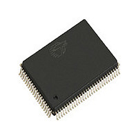
CY7C1356B-166AI Cypress Semiconductor Corp, CY7C1356B-166AI Datasheet - Page 10

CY7C1356B-166AI
Manufacturer Part Number
CY7C1356B-166AI
Description
Manufacturer
Cypress Semiconductor Corp
Datasheet
1.CY7C1356B-166AI.pdf
(29 pages)
Specifications of CY7C1356B-166AI
Density
9Mb
Access Time (max)
3.5ns
Sync/async
Synchronous
Architecture
SDR
Clock Freq (max)
166MHz
Operating Supply Voltage (typ)
3.3V
Address Bus
19b
Package Type
TQFP
Operating Temp Range
-40C to 85C
Number Of Ports
1
Supply Current
180mA
Operating Supply Voltage (min)
3.135V
Operating Supply Voltage (max)
3.465V
Operating Temperature Classification
Industrial
Mounting
Surface Mount
Pin Count
100
Word Size
18b
Number Of Words
512K
Lead Free Status / Rohs Status
Not Compliant
Available stocks
Company
Part Number
Manufacturer
Quantity
Price
Part Number:
CY7C1356B-166AI
Manufacturer:
CYPRESS/赛普拉斯
Quantity:
20 000
Document #: 38-05114 Rev. *C
IEEE 1149.1 Serial Boundary Scan (JTAG)
The CY7C1354B/CY7C1354B incorporates a serial boundary
scan Test Access Port (TAP) in the BGA package only. The
TQFP package does not offer this functionality. This port
operates in accordance with IEEE Standard 1149.1-1900, but
does not have the set of functions required for full 1149.1
compliance. These functions from the IEEE specification are
excluded because their inclusion places an added delay in the
critical speed path of the SRAM. Note that the TAP controller
functions in a manner that does not conflict with the operation
of other devices using 1149.1 fully compliant TAPs. The TAP
operates using JEDEC standard 3.3V I/O logic levels.
Disabling the JTAG Feature
It is possible to operate the SRAM without using the JTAG
feature. To disable the TAP controller, TCK must be tied LOW
(V
nally pulled up and may be unconnected. They may alternately
be connected to V
be left unconnected. Upon power-up, the device will come up
in a reset state which will not interfere with the operation of the
device.
Read
Write –No bytes written
Write Byte a– (DQ
Write Byte b – (DQ
Write Bytes b, a
Write Byte c – (DQ
Write Bytes c, a
Write Bytes c, b
Write Bytes c, b, a
Write Byte d – (DQ
Write Bytes d, a
Write Bytes d, b
Write Bytes d, b, a
Write Bytes d, c
Write Bytes d, c, a
Write Bytes d, c, b
Write All Bytes
Note:
Read
Write – No Bytes Written
Write Byte a − (DQ
Write Byte b – (DQ
Write Both Bytes
Partial Write Cycle Description
8. Table only lists a partial listing of the byte write combinations. Any combination of BW
SS
) to prevent clocking of the device. TDI and TMS are inter-
Function (CY7C1354B)
a
DD
c
d
a
b
b
and DQP
and DQP
and DQP
and DQP
and DQP
and DQP
through a pull-up resistor. TDO should
Function (CY7C1356B)
a)
c)
a)
b)
d)
b)
[1, 2, 3, 8]
WE
H
L
L
L
L
L
L
L
L
L
L
L
L
L
L
L
L
Test Access Port–Test Clock
The test clock is used only with the TAP controller. All inputs
are captured on the rising edge of TCK. All outputs are driven
from the falling edge of TCK.
Test Mode Select
The TMS input is used to give commands to the TAP controller
and is sampled on the rising edge of TCK. It is allowable to
leave this pin unconnected if the TAP is not used. The pin is
pulled up internally, resulting in a logic HIGH level.
Test Data-In (TDI)
The TDI pin is used to serially input information into the
registers and can be connected to the input of any of the
registers. The register between TDI and TDO is chosen by the
instruction that is loaded into the TAP instruction register. For
information on loading the instruction register, see the TAP
Controller State Diagram. TDI is internally pulled up and can
be unconnected if the TAP is unused in an application. TDI is
connected to the Most Significant Bit (MSB) on any register.
Test Data Out (TDO)
The TDO output pin is used to serially clock data-out from the
registers. The output is active depending upon the current
state of the TAP state machine (see TAP Controller State
[a:d]
is valid. Appropriate write will be done based on which byte write is active.
BW
X
H
H
H
H
H
H
H
H
L
L
L
L
L
L
L
L
d
WE
H
L
L
L
L
BW
H
H
H
H
H
H
H
H
X
L
L
L
L
L
L
L
L
c
BW
H
H
x
L
L
b
BW
X
H
H
H
H
H
H
H
H
L
L
L
L
L
L
L
L
CY7C1356B
CY7C1354B
b
Page 10 of 29
BW
H
H
L
x
L
BW
a
X
H
H
H
H
H
H
H
H
L
L
L
L
L
L
L
L
a
[+] Feedback


