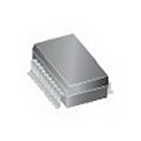
ICS8725AM-21 IDT, Integrated Device Technology Inc, ICS8725AM-21 Datasheet

ICS8725AM-21
Specifications of ICS8725AM-21
Available stocks
Related parts for ICS8725AM-21
ICS8725AM-21 Summary of contents
Page 1
... Industrial temperature information available upon request Pin Assignment QFB 1 nQFB 7.5mm x 12.8mm x 2.3mm package body 1 ICS8725-21 CLK nCLK 2 19 SEL1 SEL0 nFB_IN 5 16 PLL_SEL FB_IN DDA SEL2 SEL3 7 14 GND 8 13 nQFB QFB ICS8725-21 20-Lead SOIC M Package Top View ICS8725AM-21 REV. A FEBRUARY 27, 2008 ...
Page 2
... Analog supply pin. PLL select. Selects between the PLL and reference clock as the input to the Pullup dividers. When LOW, selects reference clock. When HIGH, selects PLL. LVCMOS/LVTTL interface levels. No connect. Test Conditions 2 Minimum Typical Maximum ICS8725AM-21 REV. A FEBRUARY 27, 2008 Units pF Ω k Ω k ...
Page 3
... Outputs PLL_SEL = 1 PLL Enable Mode Q/nQ ÷1 ÷1 ÷1 ÷1 ÷2 ÷2 ÷2 ÷4 ÷4 ÷ ICS8725AM-21 REV. A FEBRUARY 27, 2008 ...
Page 4
... Inputs SEL3 SEL2 SEL1 IDT™ / ICS™ HSTL ZERO DELAY CLOCK GENERATOR Outputs PLL_SEL = 0 PLL Bypass Mode SEL0 Q/nQ, QFB/nQFB 0 ÷4 1 ÷4 0 ÷4 1 ÷8 0 ÷8 1 ÷8 0 ÷16 1 ÷16 0 ÷32 1 ÷64 0 ÷2 1 ÷2 0 ÷4 1 ÷1 0 ÷2 1 ÷1 4 ICS8725AM-21 REV. A FEBRUARY 27, 2008 ...
Page 5
... T = 0°C to 70°C A Typical Maximum 3.3 3.465 3.3 3.465 1.6 1.8 2.0 137 1.8V ± 0.2V 0°C to 70°C A Minimum Typical Maximum 0.3 DD -0.3 0.8 150 5 -5 -150 ICS8725AM-21 REV. A FEBRUARY 27, 2008 Units Units V V µA µA µA µA ...
Page 6
... GND + 0 1.8V ± 0.2V 0°C to 70°C A Minimum Typical Maximum 1 0.6 = 1.8V ± 0.2V 0°C to 70°C DDO A Minimum Typical Maximum 31.25 ICS8725AM-21 REV. A FEBRUARY 27, 2008 Units 150 µA 5 µA µA µA 1.3 V – 0. Units 1 1.1 V Units ...
Page 7
... V = 1.8V ± 0.2V, T DDA DDO Test Conditions PLL_SEL = 0V, f ≤ 700MHz PLL_SEL = 3.3V PLL_SEL = 0V 20 0°C to 70°C A Minimum Typical Maximum 630 3.2 4.5 -95 30 155 50 35 ±50 1 300 700 PERIOD PERIOD PERIOD ICS8725AM-21 REV. A FEBRUARY 27, 2008 Units MHz ...
Page 8
... V DD SCOPE Qx nCLK CLK nQx GND Differential Input Level nQx nQy = Phase Jitter Qy is the average mean Output Skew nQ, nQFB Q, QFB tcycle n+1 Output Pulse Width Cross Points PP tsk( DDO DDO 2 2 Pulse Width t PERIOD ICS8725AM-21 REV. A FEBRUARY 27, 2008 CMR V DDO 2 ...
Page 9
... V pin. The 10Ω resistor can also be replaced by a ferrite bead. DDA IDT™ / ICS™ HSTL ZERO DELAY CLOCK GENERATOR nCLK 80% CLK nQ, nQFB 20 QFB F Propagation Delay 3. .01µ DDA .01µF 10µF Figure 1. Power Supply Filtering ICS8725AM-21 REV. A FEBRUARY 27, 2008 ...
Page 10
... For example, if the input clock swing is only 2.5V and V = 3.3V, V_REF should be 1.25V and DD R2/R1 = 0.609. IDT™ / ICS™ HSTL ZERO DELAY CLOCK GENERATOR / CLK_IN C1 0.1uF Figure 2. Single-Ended Signal Driving Differential Input V_REF - R2 1K ICS8725AM-21 REV. A FEBRUARY 27, 2008 ...
Page 11
... R2 50 Driven by a 3.3V LVPECL Driver 100 LVDS Driven by a 3.3V LVDS Driver 2. 120 120 SSTL R1 R2 120 120 Driven by a 2.5V SSTL Driver ICS8725AM-21 REV. A FEBRUARY 27, 2008 3.3V CLK nCLK HiPerClockS Input 3.3V CLK nCLK Receiver 3.3V CLK nCLK HiPerClockS ...
Page 12
... VDDO=1.8V SEL[3:0] = 0101, Divide VDDA 10 20 C11 nc SEL1 19 0.01u C16 SEL0 18 10u VDD 17 PLL_SEL 16 VDDA 15 SEL3 14 VDDO Ohm Ohm 0.1uF (77.75 MHz Bypass capacitors located near the power pins (U1-4) VDD (U1-17 0.1uF 0.1uF ICS8725AM-21 REV. A FEBRUARY 27, 2008 VDD + - LVHSTL_input R5 50 ...
Page 13
... DD )= 3.465V * (137mA + 17mA) = 533.6mW * ( DD_MAX DDA_MAX * Pd_total + for 20 Lead SOIC, Forced Convection θ vs. Air Flow JA 0 83.2°C/W 46.2°C/W 13 must be used. Assuming a moderate JA 200 500 65.7°C/W 57.5°C/W 39.7°C/W 36.8°C/W ICS8725AM-21 REV. A FEBRUARY 27, 2008 ...
Page 14
... V OH_MAX DDO_MAX L Pd_L = ( OL_MAX DDO_MAX L Pd_H = (1.0V/50Ω) * (2V - 1.0V) = 20mW Pd_L = (0.4V/50Ω) * (2V - 0.4V) = 12.8mW Total Power Dissipation per output pair = Pd_H + Pd_L = 32.8mW IDT™ / ICS™ HSTL ZERO DELAY CLOCK GENERATOR V OUT OH_MAX ) OL_MAX 14 ICS8725AM-21 REV. A FEBRUARY 27, 2008 ...
Page 15
... Symbol Minimum 0.10 A2 2.05 B 0.33 C 0.18 D 12.60 E 7.40 e 1.27 Basic H 10.00 h 0.25 L 0.40 α 0° Reference Document: JEDEC Publication 95, MS-013, MS-119 15 ICS8725AM-21 REV. A FEBRUARY 27, 2008 500 57.5°C/W 36.8°C/W Maximum 2.65 2.55 0.51 0.32 13.00 7.60 10.65 0.75 1.27 8° ...
Page 16
... Shipping Packaging 20 Lead SOIC 20 Lead SOIC 1000 Tape & Reel “Lead-Free” 20 Lead SOIC “Lead-Free” 20 Lead SOIC 1000 Tape & Reel 16 Temperature Tube 0°C to 70°C 0°C to 70°C Tube 0°C to 70°C 0°C to 70°C ICS8725AM-21 REV. A FEBRUARY 27, 2008 ...
Page 17
... Pin Descriptions Table - corrected MR description Added Recommendations for Unused Input and Output Pins. 11 Updated Differential Clock Input Interface section Updated Schematic Example section. IDT™ / ICS™ HSTL ZERO DELAY CLOCK GENERATOR Description of Change 17 ICS8725AM-21 REV. A FEBRUARY 27, 2008 Date 6/9/05 5/22/06 2/27/08 ...
Page 18
ICS8725-21 DIFFERENTIAL-TO-HSTL ZERO DELAY CLOCK GENERATOR Innovate with IDT and accelerate your future networks. Contact: www.IDT.com For Sales 800-345-7015 408-284-8200 Fax: 408-284-2775 Corporate Headquarters Integrated Device Technology, Inc. 6024 Silver Creek Valley Road San Jose, CA 95138 United States 800 ...


