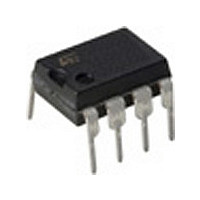
M24C01-BN6 STMicroelectronics, M24C01-BN6 Datasheet - Page 12

M24C01-BN6
Manufacturer Part Number
M24C01-BN6
Description
Manufacturer
STMicroelectronics
Datasheet
1.M24C01-BN6.pdf
(40 pages)
Specifications of M24C01-BN6
Density
1Kb
Interface Type
Serial (I2C)
Organization
128x8
Access Time (max)
900ns
Frequency (max)
400KHz
Write Protection
Yes
Data Retention
40Year
Operating Supply Voltage (typ)
5V
Package Type
PDIP
Operating Temp Range
-40C to 85C
Supply Current
2mA
Operating Supply Voltage (min)
4.5V
Operating Supply Voltage (max)
5.5V
Operating Temperature Classification
Industrial
Mounting
Through Hole
Pin Count
8
Lead Free Status / Rohs Status
Not Compliant
Available stocks
Company
Part Number
Manufacturer
Quantity
Price
Device operation
3
3.1
3.2
3.3
3.4
12/40
Device operation
The device supports the I²C protocol. This is summarized in
data on to the bus is defined to be a transmitter, and any device that reads the data to be a
receiver. The device that controls the data transfer is known as the bus master, and the
other as the slave device. A data transfer can only be initiated by the bus master, which will
also provide the serial clock for synchronization. The M24Cxx device is always a slave in all
communication.
Start condition
Start is identified by a falling edge of Serial Data (SDA) while Serial Clock (SCL) is stable in
the High state. A Start condition must precede any data transfer command. The device
continuously monitors (except during a Write cycle) Serial Data (SDA) and Serial Clock
(SCL) for a Start condition, and will not respond unless one is given.
Stop condition
Stop is identified by a rising edge of Serial Data (SDA) while Serial Clock (SCL) is stable
and driven High. A Stop condition terminates communication between the device and the
bus master. A Read command that is followed by NoAck can be followed by a Stop condition
to force the device into the Standby mode. A Stop condition at the end of a Write command
triggers the internal Write cycle.
Acknowledge bit (ACK)
The acknowledge bit is used to indicate a successful byte transfer. The bus transmitter,
whether it be bus master or slave device, releases Serial Data (SDA) after sending eight bits
of data. During the 9
acknowledge the receipt of the eight data bits.
Data input
During data input, the device samples Serial Data (SDA) on the rising edge of Serial Clock
(SCL). For correct device operation, Serial Data (SDA) must be stable during the rising edge
of Serial Clock (SCL), and the Serial Data (SDA) signal must change only when Serial Clock
(SCL) is driven Low.
th
clock pulse period, the receiver pulls Serial Data (SDA) Low to
Doc ID 5067 Rev 13
M24C16, M24C08, M24C04, M24C02, M24C01
Figure
6. Any device that sends


