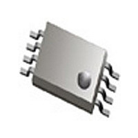
MC10EP01DT ON Semiconductor, MC10EP01DT Datasheet - Page 6

MC10EP01DT
Manufacturer Part Number
MC10EP01DT
Description
Manufacturer
ON Semiconductor
Datasheet
1.MC10EP01DT.pdf
(10 pages)
Specifications of MC10EP01DT
Logic Family
ECL
Logical Function
NOR/OR
Number Of Elements
1
High Level Output Current
-50mA
Low Level Output Current
50mA
Propagation Delay Time
0.35ns
Operating Supply Voltage (typ)
-3.3/-5/3.3/5V
Operating Temp Range
-40C to 85C
Package Type
TSSOP
Number Of Outputs
2
Number Of Inputs
4-IN
Technology
ECL
Mounting
Surface Mount
Pin Count
8
Operating Temperature Classification
Industrial
Operating Supply Voltage (max)
-5.5/5.5V
Operating Supply Voltage (min)
-3/3V
Lead Free Status / Rohs Status
Not Compliant
Available stocks
Company
Part Number
Manufacturer
Quantity
Price
Company:
Part Number:
MC10EP01DT
Manufacturer:
ON
Quantity:
1 173
Company:
Part Number:
MC10EP01DTR2
Manufacturer:
ON
Quantity:
5 000
NOTE: Device will meet the specifications after thermal equilibrium has been established when mounted in a test socket or printed circuit
15. Measured using a 750 mV source, 50% duty cycle clock source. All loading with 50 W to V
Table 11. AC CHARACTERISTICS
f
t
t
t
t
t
Symbol
max
PLH
PHL
JITTER
r
f
,
board with maintained transverse airflow greater than 500 lfpm. Electrical parameters are guaranteed only over the declared
operating temperature range. Functional operation of the device exceeding these conditions is not implied. Device specification limit
values are applied individually under normal operating conditions and not valid simultaneously.
Maximum Frequency
(See Figure 2. F
Propagation Delay
Cycle−to−Cycle Jitter
(See Figure 2. F
Output Rise/Fall Times
(20% − 80%)
Characteristic
(See Application Note AND8020/D − Termination of ECL Logic Devices.)
Figure 3. Typical Termination for Output Driver and Device Evaluation
Driver
Device
900
800
700
600
500
400
300
200
100
max
max
É É É É É É É É É É
É É É É É É É É É É
0
/JITTER)
/JITTER)
0
V
Q
Q
CC
D to Q, Q
1000
= 3.0 V to 5.5 V; V
Q, Q
2000
Min
150
50
Figure 2. F
Z
Z
http://onsemi.com
FREQUENCY (MHz)
o
o
= 50 W
= 50 W
−40°C
EE
Typ
260
120
> 3
0.2
3000
= 0 V or V
50 W
V
6
TT
max
(JITTER)
= V
Max
330
170
< 1
/Jitter
V
CC
TT
CC
4000
− 2.0 V
= 0 V; V
50 W
Min
150
60
EE
25°C
Typ
270
130
5000
> 3
0.2
= −3.0 V to −5.5 V (Note 15)
CC
D
D
− 2.0 V.
Max
330
180
< 1
6000
Receiver
Device
8
7
6
5
4
3
2
1
Min
200
70
É É
É É
É É
85°C
Typ
300
150
> 3
0.2
Max
350
200
< 1
Unit
GHz
ps
ps
ps


