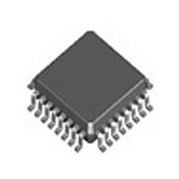
ICS8430AY-61 IDT, Integrated Device Technology Inc, ICS8430AY-61 Datasheet

ICS8430AY-61
Specifications of ICS8430AY-61
Available stocks
Related parts for ICS8430AY-61
ICS8430AY-61 Summary of contents
Page 1
G D ENERAL ESCRIPTION The ICS8430- general purpose, dual output Crystal-to-3.3V, 2.5V Differential LVPECL High Frequency Synthesizer. The ICS8430-61 has a selectable TEST_CLK or crystal inputs. The VCO operates at a frequency range of 250MHz to 500MHz. The ...
Page 2
F D UNCTIONAL ESCRIPTION NOTE: The functional description that follows describes op- eration using a 16MHz crystal. Valid PLL loop divider values for different crystal or input frequencies are defined in the In- put Frequency Characteristics, Table 5, NOTE 1. ...
Page 3
ABLE IN ESCRIPTIONS ...
Page 4
T 3A ABLE ARALLEL AND ERIAL ODE ...
Page 5
BSOLUTE AXIMUM ATINGS Supply Voltage Inputs, V -0. Outputs Continuous Current 50mA Surge Current 100mA Package Thermal Impedance, θ JA Storage Temperature, T -65°C to 150°C STG T 4A. P ...
Page 6
T 4C. LVPECL DC C ABLE HARACTERISTICS ...
Page 7
T 7A ABLE HARACTERISTICS ...
Page 8
P ARAMETER CCA, V CCO LVPECL V EE -1.3V ± 0.165V 3.3V/3. UTPUT OAD EST IRCUIT nFOUTx FOUTx nFOUTy FOUTy t sk( UTPUT KEW nFOUTx FOUTx t cycle ...
Page 9
OWER UPPLY ILTERING ECHNIQUES As in any high speed analog circuitry, the power supply pins are vulnerable to random noise. The ICS8430-61 provides separate power supplies to isolate any high switching noise from the outputs to ...
Page 10
ECOMMENDATIONS FOR NUSED I : NPUTS RYSTAL NPUT For applications not requiring the use of the crystal oscillator input, both XTAL_IN and XTAL_OUT can be left floating. Though not required, but for additional protection, ...
Page 11
T 3.3V LVPECL O ERMINATION FOR The clock layout topology shown below is a typical termina- tion for LVPECL outputs. The two different layouts mentioned are recommended only as guidelines. FOUT and nFOUT are low impedance follower outputs that generate ...
Page 12
T 2.5V LVPECL O ERMINATION FOR Figure 6A and Figure 6B show examples of termination for 2.5V LVPECL driver. These terminations are equivalent to ter- minating 50Ω 2V. For V = 2.5V, the V CC CCO 2.5V ...
Page 13
L G AYOUT UIDELINE The schematic of the ICS8430-61 layout example used in this layout guideline is shown in Figure 7A. The ICS8430-61 recommended PCB board layout for this example is shown in Figure 7B. This layout example is used ...
Page 14
The following component footprints are used in this layout example: All the resistors and capacitors are size 0603 OWER AND ROUNDING Place the decoupling capacitors C14 and C15 as close as pos- sible to the power pins. If ...
Page 15
This section provides information on power dissipation and junction temperature for the ICS8430-61. Equations and example calculations are also provided. 1. Power Dissipation. The total power dissipation for the ICS8430-61 is the sum of the core power plus the power ...
Page 16
Calculations and Equations. The purpose of this section is to derive the power dissipated into the load. LVPECL output driver circuit and termination are shown in Figure 8. F IGURE T o calculate worst case power dissipation into the ...
Page 17
ABLE VS IR LOW ABLE FOR JA Single-Layer PCB, JEDEC Standard Test Boards Multi-Layer PCB, JEDEC Standard Test Boards NOTE: Most modern PCB designs use multi-layered boards. The data in the second row ...
Page 18
ACKAGE UTLINE UFFIX FOR T 10. P ABLE ...
Page 19
T 11 ABLE RDERING NFORMATION ...
Page 20
...
Page 21
We’ve Got Your Timing Solution. 6024 Silver Creek Valley Road San Jose, CA 95138 © 2010 Integrated Device Technology, Inc. All rights reserved. Product specifications subject to change without notice. IDT, the IDT logo, ICS and HiPerClockS are trademarks of ...


