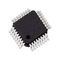
ICS8312AYI IDT, Integrated Device Technology Inc, ICS8312AYI Datasheet - Page 8

ICS8312AYI
Manufacturer Part Number
ICS8312AYI
Description
Manufacturer
IDT, Integrated Device Technology Inc
Datasheet
1.ICS8312AYI.pdf
(18 pages)
Specifications of ICS8312AYI
Number Of Outputs
12
Operating Supply Voltage (max)
3.465V
Operating Temp Range
-40C to 85C
Propagation Delay Time
4.9ns
Operating Supply Voltage (min)
1.6V
Mounting
Surface Mount
Pin Count
32
Operating Supply Voltage (typ)
1.8/2.5/3.3V
Package Type
TQFP
Duty Cycle
55%
Operating Temperature Classification
Industrial
Lead Free Status / Rohs Status
Not Compliant
Available stocks
Company
Part Number
Manufacturer
Quantity
Price
Company:
Part Number:
ICS8312AYILF
Manufacturer:
ST
Quantity:
220
Company:
Part Number:
ICS8312AYILF
Manufacturer:
IDT, Integrated Device Technology Inc
Quantity:
10 000
Company:
Part Number:
ICS8312AYILFT
Manufacturer:
IDT, Integrated Device Technology Inc
Quantity:
10 000
Table 5C. AC Characteristics, V
All parameters measured at f
NOTE 1: Measured from the V
NOTE 2: Defined as skew between outputs at the same supply voltage and with equal load conditions. Measured at V
NOTE 3: Defined as skew between outputs on different devices operating a the same supply voltage and with equal load conditions.
Using the same type of input on each device, the output is measured at V
NOTE 4: These parameters are guaranteed by characterization. Not tested in production.
NOTE 5: This parameter is defined in accordance with JEDEC Standard 65.
Table 5D. AC Characteristics, V
All parameters measured at f
NOTE 1: Measured from the V
NOTE 2: Defined as skew between outputs at the same supply voltage and with equal load conditions. Measured at V
NOTE 3: Defined as skew between outputs on different devices operating a the same supply voltage and with equal load conditions.
Using the same type of input on each device, the output is measured at V
NOTE 4: These parameters are guaranteed by characterization. Not tested in production.
NOTE 5: This parameter is defined in accordance with JEDEC Standard 65.
IDT™ / ICS™ LVCMOS/LVTTL FANOUT BUFFER
Parameter
f
tp
tjit
tsk(o)
tsk(pp)
t
odc
Parameter
f
tp
tjit
tsk(o)
tsk(pp)
t
odc
MAX
R
MAX
R
ICS8312I
LOW SKEW, 1-TO-12 LVCMOS/LVTTL FANOUT BUFFER
LH
LH
/ t
/ t
F
F
Symbol
Output Frequency
Propagation Delay, Low to High; NOTE 1
Buffer Additive Phase Jitter, RMS; refer to
Additive Phase Jitter Section
Output Skew; NOTE 2, 5
Part-to-Part Skew; NOTE 3, 5
Output Rise/Fall Time; NOTE 5
Output Duty Cycle
Symbol
Output Frequency
Propagation Delay, Low to High; NOTE 1
Buffer Additive Phase Jitter, RMS; refer to
Additive Phase Jitter Section
Output Skew; NOTE 2, 5
Part-to-Part Skew; NOTE 3, 5
Output Rise/Fall Time; NOTE 5
Output Duty Cycle
MAX
MAX
DD
DD
/2 of the input to V
/2 of the input to V
unless noted otherwise.
unless noted otherwise.
DD
DD
= V
= 3.3V ± 5%, V
DDO
= 1.8V ± 0.2V, T
DDO
DDO
/2 of the output.
/2 of the output.
DDO
= 2.5V ± 5%, T
100MHz, Integration Range:
100MHz, Integration Range:
8
A
Test Conditions
Test Conditions
12kHz – 20MHz
12kHz – 20MHz
= -40°C to 85°C
ƒ ≤ 200MHz
20% to 80%
ƒ ≤ 100MHz
ƒ ≤ 250MHz
20% to 80%
ƒ ≤ 150MHz
DDO
DDO
/2.
/2.
A
= -40°C to 85°C
Minimum Typical Maximum Units
Minimum Typical Maximum Units
175
200
1.6
1.5
45
45
ICS8312AYI REV. B JUNE 24, 2008
0.172
0.045
3.3
2.1
DDO
DDO
200
160
875
250
150
800
4.9
2.4
2.8
55
55
1
/2.
/2.
MHz
MHz
ps
ps
ns
ps
ps
ps
ns
ps
ns
ns
%
%


