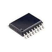
74LV4053PW NXP Semiconductors, 74LV4053PW Datasheet - Page 15

74LV4053PW
Manufacturer Part Number
74LV4053PW
Description
Multiplexer Switch ICs TRIPLE 2-CHANNEL MUX/DMUX
Manufacturer
NXP Semiconductors
Type
Analog Multiplexerr
Datasheet
1.74LV4053N112.pdf
(26 pages)
Specifications of 74LV4053PW
Number Of Channels
3 Channel
On Resistance (max)
180 Ohms
Propagation Delay Time
25 ns, 9 ns, 6 ns, 5 ns, 4 ns, 3 ns
On Time (max)
125 ns
Off Time (max)
95 ns
Supply Voltage (max)
6 V
Supply Voltage (min)
1 V
Maximum Power Dissipation
400 mW
Maximum Operating Temperature
+ 125 C
Minimum Operating Temperature
- 40 C
Package / Case
TSSOP-16
Mounting Style
SMD/SMT
Number Of Lines (input / Output)
6 / 3
Package
16TSSOP
Maximum On Resistance
435@2V Ohm
Maximum Propagation Delay Bus To Bus
25(Typ)@1.2V|9(Typ)@2V|6(Typ)@2.7V|5(Typ)@3.3V|4(Typ)@4.5V|3(Typ)@6V ns
Maximum Low Level Output Current
25 mA
Multiplexer Architecture
2:1
Maximum Turn-off Time
95(Typ)@1.2V ns
Maximum Turn-on Time
125(Typ)@1.2V ns
Power Supply Type
Single
Lead Free Status / Rohs Status
Details
Other names
74LV4053PW,112
Available stocks
Company
Part Number
Manufacturer
Quantity
Price
Company:
Part Number:
74LV4053PW
Manufacturer:
MOT
Quantity:
5 510
NXP Semiconductors
Table 11.
At recommended operating conditions; voltages are referenced to GND (ground = 0 V); V
specified); t
[1]
[2]
74LV4053_4
Product data sheet
Symbol Parameter
THD
f
V
Xtalk
( 3dB)
iso
ct
Adjust f
Adjust f
total harmonic
distortion
response
isolation (OFF-state)
crosstalk voltage
crosstalk
i
i
r
3 dB frequency
Additional dynamic characteristics
voltage to obtain 0 dBm level at output for 1 MHz (0 dBm = 1 mW into 50 ).
voltage to obtain 0 dBm level at output for 1 MHz (0 dBm = 1 mW into 600 ).
= t
f
10.2 Additional dynamic parameters
6.0 ns; T
amb
= 25 C.
Conditions
f
f
C
f
between digital inputs and switch;
f
between switches; f
R
i
i
i
i
= 1 kHz; C
= 10 kHz; C
L
= 1 MHz; C
= 1 MHz; C
L
V
V
V
V
V
V
V
V
V
V
V
V
= 50 pF; R
= 600 ; see
CC
CC
CC
CC
CC
CC
CC
CC
CC
CC
CC
CC
= 3.0 V; V
= 6.0 V; V
= 3.0 V; V
= 6.0 V; V
= 3.0 V
= 6.0 V
= 3.0 V
= 6.0 V
= 3.0 V
= 6.0 V
= 3.0 V
= 6.0 V
L
L
L
L
= 50 pF; R
L
Rev. 04 — 10 August 2009
= 50 pF; R
= 50 pF; R
= 50 pF; R
= 50 ; see
I
I
I
I
Figure 22
= 2.75 V (p-p)
= 5.5 V (p-p)
= 2.75 V (p-p)
= 5.5 V (p-p)
i
= 1 MHz; C
L
L
L
L
= 10 k ; see
= 600 ; see
= 600 ; see
= 10 k ; see
Figure 16
L
= 50 pF;
Triple single-pole double-throw analog switch
Figure 20
Figure 18
Figure 21
Figure 20
I
= GND or V
[1]
[2]
[2]
Min
-
-
-
-
-
-
-
-
-
-
-
-
74LV4053
CC
Typ
0.11
0.12
© NXP B.V. 2009. All rights reserved.
180
200
0.8
0.4
2.4
1.2
(unless otherwise
50
50
60
60
Max
-
-
-
-
-
-
-
-
-
-
-
-
15 of 26
Unit
dB
dB
MHz
MHz
dB
dB
%
%
%
%
V
V


