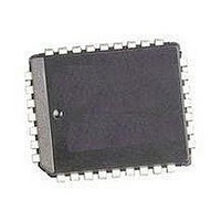
M29F010B70K1 STMicroelectronics, M29F010B70K1 Datasheet

M29F010B70K1
Specifications of M29F010B70K1
Available stocks
Related parts for M29F010B70K1
M29F010B70K1 Summary of contents
Page 1
... Mbit (128Kb x8, Uniform Block) Single Supply Flash Memory SINGLE 5V±10% SUPPLY VOLTAGE for PROGRAM, ERASE and READ OPERATIONS ACCESS TIME PROGRAMMING TIME – 8 µs per Byte typical 8 UNIFORM 16 KBytes MEMORY BLOCKS PROGRAM/ERASE CONTROLLER – Embedded Byte Program algorithm – Embedded Multi-Block/Chip Erase algorithm – ...
Page 2
M29F010B Figure 2. PLCC Connections M29F010B DQ0 17 Table 1. Signal Names A0-A16 Address Inputs DQ0-DQ7 Data Inputs/Outputs E Chip Enable G Output Enable W Write Enable V Supply ...
Page 3
... These are stress ratings only and operation of the device at these or any other conditions above those indicated in the Operating sections of this specification is not implied. Exposure to Absolute Maximum Rating condi- tions for extended periods may affect device reliability. Refer also to the STMicroelectronics SURE Program and other relevant qual- ity documents. ...
Page 4
... Disable, Standby and Automatic Standby. See Table 4, Bus Operations, for a summary. Typically glitches of less than 5ns on Chip Enable or Write Enable are ignored by the memory and do not af- fect bus operations. Bus Read. Bus Read operations read from the memory cells, or specific registers in the Com- mand Interface ...
Page 5
... Auto Select mode until another com- mand is issued. From the Auto Select mode the Manufacturer Code can be read using a Bus Read operation with and The other address bits IL IL may be set to either Code for STMicroelectronics is 20h Cell Address Command Address IH IL ...
Page 6
... Once the Unlock Bypass command has been is- sued the memory will only accept the Unlock By- pass Program command and the Unlock Bypass Reset command. The memory can be read Read mode. Unlock Bypass Program Command. The lock Bypass Program command can be used to program one address in memory at a time ...
Page 7
... Program, Unlock Bypass Program, Chip Erase, Block Erase. After these commands read the Status Register until the Program/Erase Controller completes and the memory returns to Read Mode. Add additional Blocks during Block Erase Command with additional Bus Write Operations until the Timeout Bit is set. ...
Page 8
... Bus Read operation will show the bit is still ’0’. One of the Erase commands must be used to set all the bits in a block or in the whole memory from ’0’ to ’1’. Erase Timer Bit (DQ3). The Erase Timer Bit can ...
Page 9
... Note: Unspecified data bits should be ignored. blocks being erased. Bus Read operations to ad- dresses within blocks not being erased will output the memory cell data Read mode. After an Erase operation that causes the Error Bit to be set the Alternative Toggle Bit can be used to identify which block or blocks have caused the er- ror. The Alternative Toggle Bit changes from ’ ...
Page 10
M29F010B Figure 4. Data Polling Flowchart START READ DQ5 & DQ7 at VALID ADDRESS DQ7 YES = DATA NO NO DQ5 = 1 YES READ DQ7 at VALID ADDRESS DQ7 YES = DATA NO FAIL 10/20 Figure 5. Data Toggle ...
Page 11
Table 8. AC Measurement Conditions Parameter AC Test Conditions Load Capacitance ( Input Rise and Fall Times Input Pulse Voltages Input and Output Timing Ref. Voltages Figure 6. AC Testing Input Output Waveform High Speed 3V 0V Standard ...
Page 12
M29F010B Table 10. DC Characteristics ( 70°C, –40 to 85°C or –40 to 125°C) A Symbol Parameter I Input Leakage Current LI I Output Leakage Current LO I Supply Current (Read) CC1 I Supply Current (Standby) TTL ...
Page 13
Table 11. Read AC Characteristics ( 70°C, –40 to 85°C or –40 to 125°C) Symbol Alt Parameter Address Valid to Next t t AVAV RC Address Valid t t Address Valid to Output Valid AVQV ACC Chip ...
Page 14
M29F010B Table 12. Write AC Characteristics, Write Enable Controlled ( °C, – °C or –40 to 125 °C) A Symbol Alt t t Address Valid to Next Address Valid AVAV Chip ...
Page 15
Table 13. Write AC Characteristics, Chip Enable Controlled ( °C, – °C or –40 to 125 °C) A Symbol Alt t t Address Valid to Next Address Valid AVAV Write Enable ...
Page 16
... Note: The last two characters of the ordering code may be replaced by a letter code for preprogrammed parts, otherwise devices are shipped from the factory with the memory content bits erased to ’1’. For a list of available options (Speed, Package, etc...) or for further information on any aspect of this de- vice, please contact the ST Sales Office nearest to you ...
Page 17
Table 16. PLCC32 – 32 lead Plastic Leaded Chip Carrier, Package Mechanical Data Symbol Typ 7. 10. 0.89 Figure 11. PLCC32 ...
Page 18
M29F010B Table 17. TSOP32 – 32 lead Plastic Thin Small Outline 20mm, Package Mechanical Data Symbol Typ 0. Figure 12. TSOP32 – 32 lead Plastic Thin ...
Page 19
Table 15. Revision History Date Rev. July 1999 -01 First Issue New document template Document type: from Preliminary Data to Data Sheet Status Register bit DQ5 clarification Data Polling Flowchart diagram change (Figure 4) 28-Jul-2000 -02 Data Toggle Flowchart diagram ...
Page 20
... M29F010B Information furnished is believed to be accurate and reliable. However, STMicroelectronics assumes no responsibility for the consequences of use of such information nor for any infringement of patents or other rights of third parties which may result from its use. No license is granted by implication or otherwise under any patent or patent rights of STMicroelectronics. Specifications mentioned in this publication are subject to change without notice. This publication supersedes and replaces all information previously supplied ...


