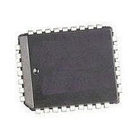
M29F010B70K1 STMicroelectronics, M29F010B70K1 Datasheet - Page 8

M29F010B70K1
Manufacturer Part Number
M29F010B70K1
Description
Flash 1M (128Kx8) 70ns
Manufacturer
STMicroelectronics
Datasheet
1.M29F010B70K1.pdf
(20 pages)
Specifications of M29F010B70K1
Data Bus Width
8 bit
Memory Type
NOR Flash
Memory Size
1 Mbit
Architecture
Sectored
Interface Type
Parallel
Supply Voltage (max)
5.5 V
Supply Voltage (min)
4.5 V
Maximum Operating Current
15 mA
Operating Temperature
+ 70 C
Mounting Style
SMD/SMT
Package / Case
PLCC-32
Organization
16 KB x 8
Lead Free Status / Rohs Status
No
Available stocks
Company
Part Number
Manufacturer
Quantity
Price
Company:
Part Number:
M29F010B70K1
Manufacturer:
CY
Quantity:
70
Part Number:
M29F010B70K1
Manufacturer:
ST
Quantity:
20 000
M29F010B
8/20
Table 6. Program, Erase Times and Program, Erase Endurance Cycles
(T
Note: 1. T
STATUS REGISTER
Bus Read operations from any address always
read the Status Register during Program and
Erase operations. It is also read during Erase Sus-
pend when an address within a block being erased
is accessed.
The bits in the Status Register are summarized in
Table 7, Status Register Bits.
Data Polling Bit (DQ7). The Data Polling Bit can
be used to identify whether the Program/Erase
Controller has successfully completed its opera-
tion or if it has responded to an Erase Suspend.
The Data Polling Bit is output on DQ7 when the
Status Register is read.
During Program operations the Data Polling Bit
outputs the complement of the bit being pro-
grammed to DQ7. After successful completion of
the Program operation the memory returns to
Read mode and Bus Read operations from the ad-
dress just programmed output DQ7, not its com-
plement.
During Erase operations the Data Polling Bit out-
puts ’0’, the complement of the erased state of
DQ7. After successful completion of the Erase op-
eration the memory returns to Read Mode.
In Erase Suspend mode the Data Polling Bit will
output a ’1’ during a Bus Read operation within a
block being erased. The Data Polling Bit will
change from a ’0’ to a ’1’ when the Program/Erase
Controller has suspended the Erase operation.
Figure 4, Data Polling Flowchart, gives an exam-
ple of how to use the Data Polling Bit. A Valid Ad-
dress is the address being programmed or an
address within the block being erased.
Toggle Bit (DQ6). The Toggle Bit can be used to
identify whether the Program/Erase Controller has
successfully completed its operation or if it has re-
sponded to an Erase Suspend. The Toggle Bit is
output on DQ6 when the Status Register is read.
Chip Erase (All bits in the memory set to ‘0’)
Chip Erase
Block Erase (16 Kbytes)
Program
Chip Program
Program/Erase Cycles (per Block)
A
= 0 to 70°C, –40 to 85°C or –40 to 125°C)
A
= 25°C, V
Parameter
CC
= 5V.
100,000
Min
During Program and Erase operations the Toggle
Bit changes from ’0’ to ’1’ to ’0’, etc., with succes-
sive Bus Read operations at any address. After
successful completion of the operation the memo-
ry returns to Read mode.
During Erase Suspend mode the Toggle Bit will
output when addressing a cell within a block being
erased. The Toggle Bit will stop toggling when the
Program/Erase Controller has suspended the
Erase operation.
Figure 5, Data Toggle Flowchart, gives an exam-
ple of how to use the Data Toggle Bit.
Error Bit (DQ5). The Error Bit can be used to
identify errors detected by the Program/Erase
Controller. The Error Bit is set to ’1’ when a Pro-
gram, Block Erase or Chip Erase operation fails to
write the correct data to the memory. If the Error
Bit is set a Read/Reset command must be issued
before other commands are issued. The Error bit
is output on DQ5 when the Status Register is read.
Note that the Program command cannot change a
bit set at ’0’ back to ’1’ and attempting to do so may
or may not set DQ5 at ‘1’. In both cases, a succes-
sive Bus Read operation will show the bit is still ’0’.
One of the Erase commands must be used to set
all the bits in a block or in the whole memory from
’0’ to ’1’.
Erase Timer Bit (DQ3). The Erase Timer Bit can
be used to identify the start of Program/Erase
Controller operation during a Block Erase com-
mand. Once the Program/Erase Controller starts
erasing the Erase Timer Bit is set to ’1’. Before the
Program/Erase Controller starts the Erase Timer
Bit is set to ’0’ and additional blocks to be erased
may be written to the Command Interface. The
Erase Timer Bit is output on DQ3 when the Status
Register is read.
Alternative Toggle Bit (DQ2). The
Toggle Bit can be used to monitor the Program/
Typ
0.6
1.3
0.3
1.2
8
(1)
100k W/E Cycles
Typical after
0.6
1.3
0.3
1.2
8
(1)
Max
150
4.5
6
2
Alternative
cycles
Unit
sec
sec
sec
sec
µs


