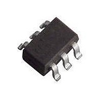
74LVC2G17GW-G NXP Semiconductors, 74LVC2G17GW-G Datasheet - Page 9

74LVC2G17GW-G
Manufacturer Part Number
74LVC2G17GW-G
Description
Buffers & Line Drivers 3.3V DUAL SCHMITT TRIGGER BUFF
Manufacturer
NXP Semiconductors
Datasheet
1.74LVC2G17GV125.pdf
(19 pages)
Specifications of 74LVC2G17GW-G
Logic Family
LVC
Logic Type
CMOS
Number Of Channels Per Chip
2
Polarity
Non-Inverting
Supply Voltage (max)
5.5 V
Supply Voltage (min)
1.65 V
Maximum Operating Temperature
+ 125 C
Mounting Style
SMD/SMT
Package / Case
SOT-363-6
High Level Output Current
- 32 mA
Low Level Output Current
32 mA
Minimum Operating Temperature
- 40 C
Number Of Lines (input / Output)
2 / 2
Propagation Delay Time
3.8 ns at 2.7 V
Lead Free Status / Rohs Status
Details
Other names
74LVC2G17GW,125
NXP Semiconductors
74LVC2G17
Product data sheet
Fig 11. Typical transfer characteristic
Fig 12. Average I
(1) Positive-going edge
(2) Negative-going edge
V
Linear change of V
CC
= 3.0 V.
CC
as a function of V
I
between 0.8 V to 2.0 V. All values given are typical unless otherwise specified.
(mA)
I
(mA)
CC
I
CC
14
12
10
50
40
30
20
10
8
6
4
2
0
0
2
0
CC
All information provided in this document is subject to legal disclaimers.
0.5
Rev. 5 — 6 August 2010
3
Dual non-inverting Schmitt trigger with 5 V tolerant input
1
4
1.5
5
(2)
(1)
V
V
CC
I
mnb071
mnb156
(V)
(V)
6
2
74LVC2G17
© NXP B.V. 2010. All rights reserved.
9 of 19


