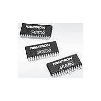
FM18L08-70-S Ramtron, FM18L08-70-S Datasheet - Page 5

FM18L08-70-S
Manufacturer Part Number
FM18L08-70-S
Description
F-RAM 256K (32Kx8) 70ns 3V
Manufacturer
Ramtron
Datasheet
1.FM18L08-70-TG.pdf
(13 pages)
Specifications of FM18L08-70-S
Memory Size
256 KB
Organization
32 K x 8
Interface
Parallel
Access Time
70 ns
Operating Supply Voltage
3 V to 3.6 V
Operating Temperature Range
- 40 C to + 85 C
Package / Case
SOIC-28
Mounting Style
SMD/SMT
Lead Free Status / Rohs Status
No
Available stocks
Company
Part Number
Manufacturer
Quantity
Price
Company:
Part Number:
FM18L08-70-S
Manufacturer:
RAMTRON
Quantity:
5 510
Part Number:
FM18L08-70-S
Manufacturer:
RAMTRON
Quantity:
20 000
Company:
Part Number:
FM18L08-70-SG
Manufacturer:
RAMTRON
Quantity:
15 040
Company:
Part Number:
FM18L08-70-SG
Manufacturer:
RAMRON
Quantity:
77
Part Number:
FM18L08-70-SG
Manufacturer:
RAMTRON
Quantity:
20 000
Company:
Part Number:
FM18L08-70-SGTR
Manufacturer:
ON
Quantity:
2 000
Part Number:
FM18L08-70-SGTR
Manufacturer:
RAMTRON
Quantity:
20 000
A second design consideration relates to the level of
V
forced to monitor V
backup. They typically block user access below a
certain V
battery with current demand from an active SRAM.
The user can be abruptly cut off from access to the
memory in a power down situation without warning.
FRAM memories do not need this system overhead.
The memory will not block access at any V
The user, however, should prevent the processor from
accessing memory when V
common design practice of holding a processor in
reset during powerdown may be sufficient. It is
recommended that Chip Enable is pulled high and
allowed to track V
cycles. It is the user’s responsibility to ensure that
chip enable is high to prevent accesses below V
min. (3.0V).
resistor on /CE which will keep the pin high during
Rev. 3.5
Sept. 2009
DD
during operation. Battery-backed SRAMs are
DD
level in order to prevent loading the
Figure 3 shows an external pullup
DD
DD
during powerup and powerdown
in order to switch to battery
DD
is out-of-tolerance. The
DD
level.
DD
power cycles assuming the MCU/MPU pin tri-states
during the reset condition. The pullup resistor value
should be chosen to ensure the /CE pin tracks V
a high enough value that the current drawn when /CE
is low is not an issue.
MCU/
Figure 3. Use of Pullup Resistor on /CE
MPU
V
R
DD
FM18L08
CE
WE
OE
A(14:0)
DQ
FM18L08
5 of 13
DD
yet


