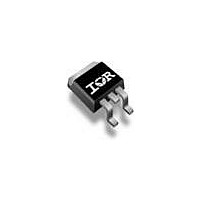
IRF9540NS International Rectifier, IRF9540NS Datasheet

IRF9540NS
Specifications of IRF9540NS
Available stocks
Related parts for IRF9540NS
IRF9540NS Summary of contents
Page 1
... Peak Diode Recovery dv/dt T Operating Junction and J T Storage Temperature Range STG Soldering Temperature, for 10 seconds Thermal Resistance Parameter R Junction-to-Case JC R Junction-to-Ambient ( PCB Mounted,steady-state)** JA IRF9540NS/L HEXFET G 2 Pak is suitable -10V GS @ -10V GS 300 (1.6mm from case ) Typ. ––– ––– 91483C ® ...
Page 2
... IRF9540NS/L Electrical Characteristics @ T Parameter V Drain-to-Source Breakdown Voltage (BR)DSS Breakdown Voltage Temp. Coefficient (BR)DSS J R Static Drain-to-Source On-Resistance DS(on) V Gate Threshold Voltage GS(th) g Forward Transconductance fs I Drain-to-Source Leakage Current DSS Gate-to-Source Forward Leakage I GSS Gate-to-Source Reverse Leakage Q Total Gate Charge g Q Gate-to-Source Charge ...
Page 3
... D rain-to-S ource V oltage ( Fig 1. Typical Output Characteristics ° 5° 0µ 0 -to-Source Volta ge ( Fig 3. Typical Transfer Characteristics IRF9540NS VGS TOP - 15V - 10V - 8.0V - 7.0V - 6.0V - 5.5V - 5.0V BOTTOM - 4. 0 rain-to-S ource V oltage ( Fig 2. Typical Output Characteristics 2 - 2.0 1.5 1.0 0.5 0.0 ...
Page 4
... IRF9540NS iss oss rss rain-to-S ourc e V oltage ( Fig 5. Typical Capacitance Vs. Drain-to-Source Voltage 5° 5° 0.1 0.2 0.4 0.6 0.8 1 ourc e-to-D rain V oltage ( Fig 7. Typical Source-Drain Diode Forward Voltage Fig 6. Typical Gate Charge Vs ing lse A 1 1.2 1.4 1.6 1 Fig 8. Maximum Safe Operating Area ...
Page 5
... Fig 11. Maximum Effective Transient Thermal Impedance, Junction-to-Case -10V Pulse Width Duty Factor Fig 10a. Switching Time Test Circuit t d(on 10% 150 175 ° 90 Fig 10b. Switching Time Waveforms Notes: 1. Duty factor Peak 0.001 0. Rectangular Pulse Duration (sec) 1 IRF9540NS D.U. µ d(off ...
Page 6
... IRF9540NS Fig 12a. Unclamped Inductive Test Circuit Fig 12b. Unclamped Inductive Waveforms Q G -10V Charge Fig 13a. Basic Gate Charge Waveform tarting unc tion T em perature (°C ) Fig 12c. Maximum Avalanche Energy V (BR)DSS 12V Fig 13b. Gate Charge Test Circuit .7A -8 .1A ...
Page 7
... D.U.T. V Waveform DS Re-Applied Voltage Body Diode Inductor Curent Ripple *** V = 5.0V for Logic Level and 3V Drive Devices GS Fig 14. For P-Channel HEXFETS IRF9540NS/L Circuit Layout Considerations Low Stray Inductance Ground Plane Low Leakage Inductance Current Transformer - + dv/dt controlled controlled by Duty Factor "D" SD D.U.T. - Device Under Test P ...
Page 8
... IRF9540NS Pak Package Outline 1 0.54 (.4 15) 1 0.29 (.4 05) 1.4 0 (.055 ) - AX. 2 1 (.6 10) 1 (.5 80 1.40 (.0 55) 3X 1.14 (.0 45) 0 .93 (. .69 (. .08 (. .25 (. FTER IP & 4.5M , 198 TRO L LIN SIO ATSINK & Part Marking Information 2 D Pak TIO 4.69 (.1 85) 4.20 (.1 65) 1 ...
Page 9
... Package Outline TO-262 Outline Part Marking Information TO-262 IRF9540NS/L ...
Page 10
... IRF9540NS/L Tape & Reel Information 2 D Pak IRE CTIO (. (. IRE C TIO N 33 0.00 (1 4 LLIN ILL WORLD HEADQUARTERS: 233 Kansas St., El Segundo, California 90245, Tel: (310) 322 3331 EUROPEAN HEADQUARTERS: Hurst Green, Oxted, Surrey RH8 9BB, UK Tel 1883 732020 IR CANADA: 7321 Victoria Park Ave., Suite 201, Markham, Ontario L3R 2Z8, Tel: (905) 475 1897 IR GERMANY: Saalburgstrasse 157, 61350 Bad Homburg Tel 6172 96590 IR FAR EAST: K& ...


