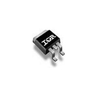
IRF9540NS International Rectifier, IRF9540NS Datasheet - Page 2

IRF9540NS
Manufacturer Part Number
IRF9540NS
Description
P CHANNEL MOSFET, -100V, 23A D2-PAK
Manufacturer
International Rectifier
Datasheet
1.IRF9540NS.pdf
(10 pages)
Specifications of IRF9540NS
Transistor Polarity
P Channel
Continuous Drain Current Id
-23A
Drain Source Voltage Vds
-100V
On Resistance Rds(on)
117mohm
Rds(on) Test Voltage Vgs
-10V
Threshold Voltage Vgs Typ
-4V
Rohs Compliant
No
Available stocks
Company
Part Number
Manufacturer
Quantity
Price
Company:
Part Number:
IRF9540NS
Manufacturer:
IR
Quantity:
1 040
Part Number:
IRF9540NS
Manufacturer:
IR
Quantity:
20 000
Company:
Part Number:
IRF9540NSPBF
Manufacturer:
IR
Quantity:
34 000
Part Number:
IRF9540NSPBF
Manufacturer:
IR
Quantity:
20 000
Company:
Part Number:
IRF9540NSTRLPBF
Manufacturer:
IR
Quantity:
34 000
Part Number:
IRF9540NSTRLPBF
Manufacturer:
INFINEON/英飞凌
Quantity:
20 000
IRF9540NS/L
Electrical Characteristics @ T
Source-Drain Ratings and Characteristics
I
I
V
t
Q
t
I
I
L
S
V
R
V
g
Q
Q
Q
t
t
t
t
C
C
C
on
DSS
SM
rr
GSS
d(on)
d(off)
f
** When mounted on 1" square PCB (FR-4 or G-10 Material ).
r
S
SD
V
fs
Notes:
rr
(BR)DSS
DS(on)
GS(th)
iss
oss
rss
gd
g
gs
(BR)DSS
For recommended footprint and soldering techniques refer to application note #AN-994.
Repetitive rating; pulse width limited by
max. junction temperature. ( See fig. 11 )
R
T
I
Starting T
SD
J
G
= 25 , I
/ T
175°C
-11A, di/dt
J
Continuous Source Current
(Body Diode)
Pulsed Source Current
(Body Diode)
Diode Forward Voltage
Reverse Recovery Time
Reverse Recovery Charge
Forward Turn-On Time
Drain-to-Source Leakage Current
Internal Source Inductance
Drain-to-Source Breakdown Voltage
Breakdown Voltage Temp. Coefficient
Static Drain-to-Source On-Resistance
Gate Threshold Voltage
Forward Transconductance
Gate-to-Source Forward Leakage
Gate-to-Source Reverse Leakage
Total Gate Charge
Gate-to-Source Charge
Gate-to-Drain ("Miller") Charge
Turn-On Delay Time
Rise Time
Turn-Off Delay Time
Fall Time
Input Capacitance
Output Capacitance
Reverse Transfer Capacitance
J
= 25°C, L = 7.1mH
AS
= -11A. (See Figure 12)
-470A/µs, V
Parameter
Parameter
DD
V
(BR)DSS
J
= 25°C (unless otherwise specified)
,
-100
Min. Typ. Max. Units
-2.0
Min. Typ. Max. Units
–––
–––
–––
–––
–––
–––
–––
–––
–––
–––
–––
–––
–––
–––
–––
–––
–––
–––
–––
–––
–––
5.3
–––
Uses IRF9540N data and test conditions
Pulse width
Intrinsic turn-on time is negligible (turn-on is dominated by L
-0.11 –––
1300 –––
–––
–––
–––
150
830 1200
–––
–––
–––
–––
––– -250
–––
––– -100
–––
–––
400
240
––– 0.117
–––
15
51
51
7.5
67
-1.6
220
-4.0
100
–––
–––
–––
–––
–––
–––
–––
–––
–––
-23
-76
-25
97
15
51
300µs; duty cycle
V/°C
nC
ns
µA
nA
ns
nH
nC
V
pF
A
V
V
S
MOSFET symbol
showing the
p-n junction diode.
T
T
di/dt = -100A/µs
integral reverse
V
Reference to 25°C, I
V
V
V
V
V
V
V
I
V
V
R
R
Between lead,
and center of die contact
V
ƒ = 1.0MHz, See Fig. 5
V
I
V
D
D
J
J
GS
GS
DS
DS
DS
DS
GS
GS
DS
GS
DD
GS
DS
G
D
= 25°C, I
= 25°C, I
= -11A
= -11A
= 5.1
= 4.2
= V
= -80V, V
= 0V, I
= -10V, I
= -50V, I
= -100V, V
= 20V
= -20V
= -80V
= -10V, See Fig. 6 and 13
= 0V
= -25V
= -50V
GS
2%.
, I
F
See Fig. 10
S
D
D
= -11A
Conditions
= -11A, V
= -250µA
D
D
GS
Conditions
= -250µA
= -11A
= -11A
GS
= 0V, T
= 0V
D
= -1mA
GS
G
J
= 0V
= 150°C
S
+L
D
S
D
)


