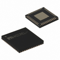
SY89540UMG Micrel Inc, SY89540UMG Datasheet - Page 4

SY89540UMG
Manufacturer Part Number
SY89540UMG
Description
IC XPOINT SWITCH 4X4 LVDS 44-MLF
Manufacturer
Micrel Inc
Series
SY89r
Datasheet
1.SY89540UMY.pdf
(14 pages)
Specifications of SY89540UMG
Function
Crosspoint Switch
Circuit
1 x 4:4
Voltage Supply Source
Single Supply
Voltage - Supply, Single/dual (±)
2.375 V ~ 2.625 V
Current - Supply
200mA
Operating Temperature
-40°C ~ 85°C
Mounting Type
Surface Mount
Package / Case
44-MLF®, QFN
Number Of Arrays
1
Differential Data Transmission
Yes
Power Supply Requirement
Single
Mounting
Surface Mount
Operating Temperature (max)
85C
Operating Temperature (min)
-40C
Operating Temperature Classification
Industrial
Cascading Capability
No
Line Code
NRZ
On-chip Buffers
No
On-chip Decoder
No
On-chip Latch Circuit
No
On-chip Mux/demux
No
Programmable
No
Dual Supply Voltage (typ)
Not RequiredV
Dual Supply Voltage (max)
Not RequiredV
Dual Supply Voltage (min)
Not RequiredV
Input Level
CML/LVDS/LVPECL
Output Level
LVDS
Lead Free Status / RoHS Status
Lead free / RoHS Compliant
Other names
576-2563
SY89540UMG
SY89540UMG
Pin Description
December 2007
Pin Number
12, 13, 20,
28, 31, 34
21,35, 36,
6, 22, 25,
17, 15,
23, 24,
26, 27,
29, 30,
41, 39
18, 19
38, 37
32, 33
43, 44
16, 9,
10, 8
3, 40
4, 2
5, 7
14,
11,
42
1,
Exposed pad
VREF_AC0,
VREF_AC1,
VREF_AC2,
VREF_AC3
Pin Name
VT0, VT1,
IN0, /IN0,
IN1, /IN1,
IN2, /IN2,
VT2, VT3
IN3, /IN3
Q0, /Q0,
Q1, /Q1,
Q2, /Q2,
Q3, /Q3,
SOUT0,
SOUT1
CONF,
LOAD
SIN0,
GND,
SIN1
VCC
Pin Function
Differential Inputs: These input pairs are the differential signal inputs to the
device. Inputs accept AC- or DC-coupled signals as small as 100mV. Each pin
of a pair internally terminates to a VT pin through 50Ω. Note that these inputs
will default to an indeterminate state if left open. Please refer to the "Input
Interface Applications" section for more details.
Input Termination Center-Tap: Each side of the differential input pair terminates
to a VT pin. The VT pins provide a center-tap to a termination network for
maximum interface flexibility. See "Input Interface Applications" section for more
details.
Reference Voltage: This output biases to V
coupling the inputs (IN, /IN). Connect VREF_AC to the VT pin. Bypass each
VREF-AC pin with a 0.01μF low ESR capacitor. See "Input Interface
Applications" section for more details.
These single-ended TTL/CMOS-compatible inputs address the data inputs.
Note that these inputs are internally connected to a 25kΩ pull-up resistor and
will default to a logic HIGH state if left open.
These single-ended TTL/CMOS-compatible inputs address the data outputs.
Note that these inputs are internally connected to a 25kΩ pull-up resistor and
will default to logic HIGH state if left open.
These single-ended TTL/CMOS-compatible inputs control the transfer of the
addresses to the internal multiplexers. See "Address Tables" and "Timing
Diagram" sections for more details. Note that these inputs are internally
connected to a 25kΩ pull-up resistor and will default to logic HIGH state if left
open.
Configuration Sequence
1. Load: Loads configuration into buffer, while Configuration Buffer holds
existing switch configuration.
2. Configuration: Loads new configuration into the Configuration Buffer and
updates switch configuration.
Buffer Mode
The SY89540U defaults to buffer mode (IN to Q) if the load and configuration
control signals are not exercised.
Differential Outputs: These LVDS output pairs are the outputs of the device.
Please refer to the truth table below for details. Unused output pairs may be left
open. Each output is designed to drive 350mV into 100Ω across the pair.
Positive power supply. Bypass with 0.1μF//0.01μF low ESR capacitors and
place as close to each V
Ground. GND and EPad must both be connected to the same ground.
4
CC
pin.
hbwhelp@micrel.com
CC
–1.2V. It is used when AC-
or (408) 955-1690
M9999-120607-C


