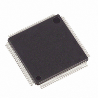
DS21354LC1+ Maxim Integrated Products, DS21354LC1+ Datasheet - Page 22

DS21354LC1+
Manufacturer Part Number
DS21354LC1+
Description
IC TXRX E1 3.3V 100-LQFP
Manufacturer
Maxim Integrated Products
Datasheet
1.DS2154LNA2.pdf
(124 pages)
Specifications of DS21354LC1+
Function
Single-Chip Transceiver
Interface
E1, HDLC
Number Of Circuits
1
Voltage - Supply
3.14 V ~ 3.47 V
Current - Supply
75mA
Operating Temperature
0°C ~ 70°C
Mounting Type
Surface Mount
Package / Case
100-LQFP
Includes
Remote and AIS Alarm Detector / Generator
Lead Free Status / RoHS Status
Lead free / RoHS Compliant
Power (watts)
-
- Current page: 22 of 124
- Download datasheet (945Kb)
3.1.4.
Signal Name:
Signal Description:
Signal Type:
This signal is used to asynchronously reset the test access port controller. At power up, JTRST must be
toggled from low to high. This action will set the device into JTAG DEVICE ID mode enabling the test
access port features. This pin has a 10kW pullup resistor. When FMS = 1, this pin is tied low internally.
Tie JTRST low if JTAG is not used and the framer is in DS21354/DS21554 mode (FMS low).
Signal Name:
Signal Description:
Signal Type:
This pin is sampled on the rising edge of JTCLK and is used to place the test access port into the various
defined IEEE 1149.1 states. This pin has a 10kW pullup resistor.
Signal Name:
Signal Description:
Signal Type:
This signal is used to shift data into JTDI on the rising edge and out of JTDO on the falling edge.
Signal Name:
Signal Description:
Signal Type:
Test instructions and data are clocked into this pin on the rising edge of JTCLK. This pin has a 10kW
pullup resistor.
Signal Name:
Signal Description:
Signal Type:
Test instructions and data are clocked out of this pin on the falling edge of JTCLK. If not used, this pin
should be left unconnected.
3.1.5.
Signal Name:
Signal Description:
Signal Type:
A rising edge on this pin causes RSER and RSIG to come out of high-Z state and TSER and TSIG to start
sampling on the next rising edge of RSYSCLK/TSYSCLK beginning an I/O sequence of 8 or 256 bits of
data. This pin has a 10kW pullup resistor.
Signal Name:
Signal Description:
Signal Type:
An output that is set high when the last bit of the 8 or 256 IBO output sequence has occurred on RSER
and RSIG.
JTAG Test Access Port Pins
Interleave Bus Operation Pins
JTRST
IEEE 1149.1 Test Reset
Input
JTMS
IEEE 1149.1 Test Mode Select
Input
JTCLK
IEEE 1149.1 Test Clock Signal
Input
JTDI
IEEE 1149.1 Test Data Input
Input
JTDO
IEEE 1149.1 Test Data Output
Output
CI
Carry In
Input
CO
Carry Out
Output
22 of 124
Related parts for DS21354LC1+
Image
Part Number
Description
Manufacturer
Datasheet
Request
R

Part Number:
Description:
Manufacturer:
Maxim Integrated Products
Datasheet:

Part Number:
Description:
power light source Luxeon Line
Manufacturer:
LUMILEDS [Lumileds Lighting Company]
Datasheet:

Part Number:
Description:
MAX7528KCWPMaxim Integrated Products [CMOS Dual 8-Bit Buffered Multiplying DACs]
Manufacturer:
Maxim Integrated Products
Datasheet:

Part Number:
Description:
Single +5V, fully integrated, 1.25Gbps laser diode driver.
Manufacturer:
Maxim Integrated Products
Datasheet:

Part Number:
Description:
Single +5V, fully integrated, 155Mbps laser diode driver.
Manufacturer:
Maxim Integrated Products
Datasheet:

Part Number:
Description:
VRD11/VRD10, K8 Rev F 2/3/4-Phase PWM Controllers with Integrated Dual MOSFET Drivers
Manufacturer:
Maxim Integrated Products
Datasheet:

Part Number:
Description:
Highly Integrated Level 2 SMBus Battery Chargers
Manufacturer:
Maxim Integrated Products
Datasheet:

Part Number:
Description:
Current Monitor and Accumulator with Integrated Sense Resistor; ; Temperature Range: -40°C to +85°C
Manufacturer:
Maxim Integrated Products

Part Number:
Description:
TSSOP 14/A°/RS-485 Transceivers with Integrated 100O/120O Termination Resis
Manufacturer:
Maxim Integrated Products

Part Number:
Description:
TSSOP 14/A°/RS-485 Transceivers with Integrated 100O/120O Termination Resis
Manufacturer:
Maxim Integrated Products

Part Number:
Description:
QFN 16/A°/AC-DC and DC-DC Peak-Current-Mode Converters with Integrated Step
Manufacturer:
Maxim Integrated Products

Part Number:
Description:
TDFN/A/65V, 1A, 600KHZ, SYNCHRONOUS STEP-DOWN REGULATOR WITH INTEGRATED SWI
Manufacturer:
Maxim Integrated Products

Part Number:
Description:
Integrated Temperature Controller f
Manufacturer:
Maxim Integrated Products

Part Number:
Description:
SOT23-6/I°/45MHz to 650MHz, Integrated IF VCOs with Differential Output
Manufacturer:
Maxim Integrated Products


