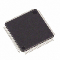
DS21354LC1+ Maxim Integrated Products, DS21354LC1+ Datasheet - Page 57

DS21354LC1+
Manufacturer Part Number
DS21354LC1+
Description
IC TXRX E1 3.3V 100-LQFP
Manufacturer
Maxim Integrated Products
Datasheet
1.DS2154LNA2.pdf
(124 pages)
Specifications of DS21354LC1+
Function
Single-Chip Transceiver
Interface
E1, HDLC
Number Of Circuits
1
Voltage - Supply
3.14 V ~ 3.47 V
Current - Supply
75mA
Operating Temperature
0°C ~ 70°C
Mounting Type
Surface Mount
Package / Case
100-LQFP
Includes
Remote and AIS Alarm Detector / Generator
Lead Free Status / RoHS Status
Lead free / RoHS Compliant
Power (watts)
-
Each Receive Signaling Register (RS1 to RS16) reports the incoming signaling from two time slots. The
bits in the Receive Signaling Registers are updated on multiframe boundaries so the user can utilize the
Receive Multiframe Interrupt in the Receive Status Register 2 (SR2.7) to know when to retrieve the
signaling bits. The user has a full 2ms to retrieve the signaling bits before the data is lost. The RS
registers are updated under all conditions. Their validity should be qualified by checking for
synchronization at the CAS level. In CCS signaling mode, RS1 to RS16 can also be used to extract
signaling information. Via the SR2.7 bit, the user will be informed when the signaling registers have been
loaded with data. The user has 2ms to retrieve the data before it is lost. The signaling data reported in
RS1 to RS16 is also available at the RSIG and RSER pins.
A change in the signaling bits from one multiframe to the next causes the RSA1 (SR1.7) and RSA0
(SR1.5) status bits to be set at the same time. The user can enable the INT pin to toggle low upon
detection of a change in signaling by setting either the IMR1.7 or IMR1.5 bit. Once a signaling change
has been detected, the user has at least 1.75ms to read the data out of the RS1 to RS16 registers before the
data is lost.
TS1 TO TS16: TRANSMIT SIGNALING REGISTERS (Address = 40 to 4F Hex)
(MSB)
Each Transmit Signaling Register (TS1 to TS16) contains the CAS bits for two time slots that will be
inserted into the outgoing stream if enabled to do so via TCR1.5. On multiframe boundaries, the framer
will load the values present in the Transmit Signaling Register into an outgoing signaling shift register
that is internal to the device. The user can utilize the Transmit Multiframe bit in Status Register 2 (SR2.5)
to know when to update the signaling bits. The bit will be set every 2ms, and the user has 2ms to update
SYMBOL
A(10)
A(11)
A(12)
A(13)
A(14)
A(15)
A(1)
A(2)
A(3)
A(4)
A(5)
A(6)
A(7)
A(8)
A(9)
D(30)
0
A(1)
X
Y
B(10)
B(11)
B(12)
B(13)
B(14)
B(15)
B(1)
B(2)
B(3)
B(4)
B(5)
B(6)
B(7)
B(8)
B(9)
0
POSITION
TS1.0/1/3
TS2.7 1.
TS16.0
TS1.2
C(10)
C(11)
C(12)
C(13)
C(14)
C(15)
C(1)
C(2)
C(3)
C(4)
C(5)
C(6)
B(7)
C(8)
C(9)
0
Spare Bits
Remote Alarm Bit (integrated and reported in SR1.6)
Signaling Bit A for Channel 1
Signaling Bit D for Channel 30
D(10)
D(11)
D(12)
D(13)
D(14)
D(15)
D(1)
D(2)
D(3)
D(4)
D(5)
D(6)
D(8)
D(9)
B(7)
0
A(16)
A(17)
A(18)
A(19)
A(20)
A(21)
A(23)
A(24)
A(25)
A(26)
A(27)
A(28)
A(29)
A(30)
B(22)
X
57 of 124
NAME AND DESCRIPTION
B(16)
B(17)
B(18)
B(19)
B(20)
B(21)
B(22)
B(23)
B(24)
B(25)
B(26)
B(27)
B(28)
B(29)
B(30)
Y
C(16)
C(17)
C(18)
C(19)
C(20)
C(21)
C(23)
C(24)
C(25)
C(26)
C(27)
C(28)
C(29)
C(30)
B(22)
X
(LSB)
D(16)
D(17)
D(18)
D(19)
D(20)
D(21)
D(23)
D(24)
D(25)
D(26)
D(27)
D(28)
D(29)
D(30)
B(22)
X
TS1 (40)
TS2 (41)
TS3 (42)
TS4 (43)
TS5 (44)
TS6 (45)
TS7 (46)
TS8 (47)
TS9 (48)
TS10 (49)
TS11 (4A)
TS12 (4B)
TS13 (4C)
TS14 (4D)
TS15 (4E)
TS16 (4F)


