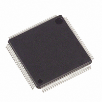
DS2156L+ Maxim Integrated Products, DS2156L+ Datasheet - Page 190

DS2156L+
Manufacturer Part Number
DS2156L+
Description
IC TXRX T1/E1/J1 1-CHIP 100-LQFP
Manufacturer
Maxim Integrated Products
Datasheet
1.DS2156L.pdf
(265 pages)
Specifications of DS2156L+
Function
Single-Chip Transceiver
Interface
E1, J1, T1, TDM, UTOPIA II
Number Of Circuits
1
Voltage - Supply
3.14 V ~ 3.47 V
Current - Supply
75mA
Operating Temperature
0°C ~ 70°C
Mounting Type
Surface Mount
Package / Case
100-LQFP
Includes
BERT Generator and Detector, CMI Coder and Decoder, HDLC Controller
Lead Free Status / RoHS Status
Lead free / RoHS Compliant
Power (watts)
-
- Current page: 190 of 265
- Download datasheet (2Mb)
Register Name:
Register Description:
Register Address:
Bit #
Name
Default
Bit 0/Receive FIFO Overrun Interrupt Status (FOIS). Set if the receive FIFO overruns provided RxFIFO
overrun interrupt mask bit (U_RCR2.3) is set. This bit is reset when read.
Bit 1/LCD Change-of-State Interrupt Status (LCDCSIS). Set by hardware if LCD status changes, provided that
the LCD interrupt-mask bit (U_RCR2.4) is set. The LCDS bit indicates the current status of LCD. This bit is reset
when read.
Bit 2/LCD Status (LCDS)
Bit 3/Receiver Mode Status (RMS). This bit shows valid status only when HEC correction is enabled.
Bits 4, 5/Cell Delineation Status 0 to 1 (CDS0 to CDS1). Bit 5 indicates instantaneous OCD status.
Bits 6, 7/Unused
Once a read cycle to this register is detected, the interrupt status bits are cleared. If any of the lower two bits is set,
the external interrupt signal is asserted. If both the bits are 0 for all the ports, the external interrupt signal is de-
asserted.
CDS1
0
0
1
0 = in-cell delineation
1 = loss-of-cell delineation
0 = correction mode
1 = detection mode
CDS0
0
1
x
—
7
0
HUNT State
PRESYNC State
SYNC State
Cell Delineation Status
—
U_RSR
UTOPIA Receive Status Register
68h
6
0
CDS1
5
0
CDS0
4
0
190 of 265
RMS
3
0
LCDS
2
1
LCDCSIS
1
0
FOIS
0
0
Related parts for DS2156L+
Image
Part Number
Description
Manufacturer
Datasheet
Request
R

Part Number:
Description:
Ds2156, Ds2156l, Ds2156ln T1/e1/j1 Single-chip Transceiver Tdm/utopia Ii Interface
Manufacturer:
Maxim Integrated Products, Inc.
Datasheet:

Part Number:
Description:
MAX7528KCWPMaxim Integrated Products [CMOS Dual 8-Bit Buffered Multiplying DACs]
Manufacturer:
Maxim Integrated Products
Datasheet:

Part Number:
Description:
Single +5V, fully integrated, 1.25Gbps laser diode driver.
Manufacturer:
Maxim Integrated Products
Datasheet:

Part Number:
Description:
Single +5V, fully integrated, 155Mbps laser diode driver.
Manufacturer:
Maxim Integrated Products
Datasheet:

Part Number:
Description:
VRD11/VRD10, K8 Rev F 2/3/4-Phase PWM Controllers with Integrated Dual MOSFET Drivers
Manufacturer:
Maxim Integrated Products
Datasheet:

Part Number:
Description:
Highly Integrated Level 2 SMBus Battery Chargers
Manufacturer:
Maxim Integrated Products
Datasheet:

Part Number:
Description:
Current Monitor and Accumulator with Integrated Sense Resistor; ; Temperature Range: -40°C to +85°C
Manufacturer:
Maxim Integrated Products

Part Number:
Description:
TSSOP 14/A�/RS-485 Transceivers with Integrated 100O/120O Termination Resis
Manufacturer:
Maxim Integrated Products

Part Number:
Description:
TSSOP 14/A�/RS-485 Transceivers with Integrated 100O/120O Termination Resis
Manufacturer:
Maxim Integrated Products

Part Number:
Description:
QFN 16/A�/AC-DC and DC-DC Peak-Current-Mode Converters with Integrated Step
Manufacturer:
Maxim Integrated Products

Part Number:
Description:
TDFN/A/65V, 1A, 600KHZ, SYNCHRONOUS STEP-DOWN REGULATOR WITH INTEGRATED SWI
Manufacturer:
Maxim Integrated Products

Part Number:
Description:
Integrated Temperature Controller f
Manufacturer:
Maxim Integrated Products

Part Number:
Description:
SOT23-6/I�/45MHz to 650MHz, Integrated IF VCOs with Differential Output
Manufacturer:
Maxim Integrated Products

Part Number:
Description:
SOT23-6/I�/45MHz to 650MHz, Integrated IF VCOs with Differential Output
Manufacturer:
Maxim Integrated Products

Part Number:
Description:
EVALUATION KIT/2.4GHZ TO 2.5GHZ 802.11G/B RF TRANSCEIVER WITH INTEGRATED PA
Manufacturer:
Maxim Integrated Products


