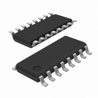
SI3200-FS Silicon Laboratories Inc, SI3200-FS Datasheet - Page 69

SI3200-FS
Manufacturer Part Number
SI3200-FS
Description
IC LINEFEED INTRFC 100V 16SOIC
Manufacturer
Silicon Laboratories Inc
Series
ProSLIC®r
Specifications of SI3200-FS
Package / Case
16-SOIC (3.9mm Width)
Function
Subscriber Line Interface Concept (SLIC), CODEC
Interface
GCI, PCM, SPI
Number Of Circuits
2
Voltage - Supply
3.3V, 5V
Current - Supply
110µA
Power (watts)
941mW
Operating Temperature
-40°C ~ 85°C
Mounting Type
Surface Mount
Includes
Battery Switching, BORSCHT Functions, DTMF Generation and Decoding, FSK Tone Generation, Modem and Fax Tone Detection
Product
SLIC
Supply Voltage (min)
3.13 V
Supply Current
0.11 mA, 8.8 mA
Maximum Operating Temperature
+ 70 C
Minimum Operating Temperature
0 C
Mounting Style
SMD/SMT
Number Of Channels
2
Lead Free Status / RoHS Status
Lead free / RoHS Compliant
Available stocks
Company
Part Number
Manufacturer
Quantity
Price
Part Number:
SI3200-FS
Manufacturer:
SILICON LABS/芯科
Quantity:
20 000
Company:
Part Number:
SI3200-FSR
Manufacturer:
SILICON
Quantity:
11 430
See Table 40 for bit definitions.
the CS pin. CS must be asserted before the falling
edge of SCLK on which the first bit of data is
expected during a read cycle and must remain low
for the duration of the 8-bit transfer (command/
address or data), going high after the last rising of
SCLK after the transfer.
Clock during transfer only . In this mode, the clock
is cycling only during the actual byte transfers. Each
byte transfer consists of eight clock cycles in a return
to “1” format.
SDI/SDO wired operation . Independent of the
clocking options described, SDI and SDO can be
3:0
7
6
5
4
BRDCST
REG/RAM Register/RAM Access Bit.
Reserved
BRDCST Indicates a broadcast operation that is intended for all devices in the daisy chain. This is
CID[3:0]
7
R/W
only valid for write operations since it would cause contention on the SDO pin during a
read.
Read/Write Bit.
0 = Write operation.
1 = Read operation.
0 = RAM access.
1 = Register access.
Indicates the channel that is targeted by the operation. Note that the 4-bit channel value is
provided LSB first. The devices reside on the daisy chain such that device 0 is nearest to
the controller, and device 15 is furthest down the SDI/SDU_THRU chain. (See Figure 41.)
As the CID information propagates down the daisy chain, each channel decrements the
CID by 1. The SDI nodes between devices reflect a decrement of 2 per device since each
device contains two channels. The device receiving a value of 0 in the CID field responds
to the SPI transaction. (See Figure 42.) If a broadcast to all devices connected to the chain
is requested, the CID does not decrement. In this case, the same 8-bit or 16-bit data is pre-
sented to all channels regardless of the CID values.
R/W
6
REG/RAM Reserved
5
Table 40. SPI Control Interface
4
Rev. 1.0
The control byte has the following structure and is
presented on the SDI pin MSB first.
CID[0]
treated as two separate lines or wired together if the
master is capable of tri-stating its output during the
data byte transfer of a read operation.
Soft reset . The SPI state machine resets whenever
CS asserts during an operation on an SCLK cycle
that is not a multiple of eight. This is a mechanism
for the controller to force the state machine to a
known state when the controller and the device are
out of synchronization.
3
CID[1]
2
Si3220/Si3225
CID[2]
1
CID[3]
0
69


