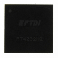
FT4232HQ - REEL FTDI, Future Technology Devices International Ltd, FT4232HQ - REEL Datasheet - Page 22

FT4232HQ - REEL
Manufacturer Part Number
FT4232HQ - REEL
Description
IC USB UART/MPSSE QUAD HS 64-QFN
Manufacturer
FTDI, Future Technology Devices International Ltd
Series
USBmadeEZ-FIFOr
Datasheet
1.FT4232HL_-_REEL.pdf
(45 pages)
Specifications of FT4232HQ - REEL
Features
USB to UART and/or SPI, I2C, JTAG
Number Of Channels
4, QUART
Fifo's
2048 Byte
Protocol
RS-232, RS-422, RS-485
Voltage - Supply
3 V ~ 3.6 V
With Auto Flow Control
Yes
With Modem Control
Yes
With Cmos
Yes
Mounting Type
Surface Mount
Package / Case
64-QFN
For Use With
768-1031 - MOD USB HS FT4232H EVAL
Lead Free Status / RoHS Status
Lead free / RoHS Compliant
Other names
768-1027-2
FT4232HQ - REEL
FT4232HQ - REEL
Document No.: FT_000060
FT4232H QUAD HIGH SPEED USB TO MULTIPURPOSE UART/MPSSE IC
Datasheet Version 2.10
Clearance No.: FTDI#78
4.5 Synchronous and Asynchronous Bit-Bang Interface Mode
Description
The FT4232H channel A,B,C or channel D can be configured as a bit-bang interface. There are two types
of bit-bang modes: synchronous and asynchronous.
Asynchronous Bit-Bang Mode
Asynchronous Bit-Bang mode is the same as BM-style Bit-Bang mode. On any channel configured in
asynchronous bit-bang mode. Data written to the device in the normal manner will be self clocked onto
the parallel I/O data pins (those which have been configured as outputs). Each I/O pin can be
independently set as an input or an output. The rate that the data is clocked out at is controlled by the
baud rate generator.
For the data to change there has to be new data written, and the baud rate clock has to tick. If no new
data is written to the channel, the pins will hold the last value written.
Synchronous Bit-Bang Mode
The synchronous Bit-Bang mode will only update the output parallel I/O port pins whenever
data is sent from the USB interface to the parallel interface. When this is done, data is read from the USB
Rx FIFO buffer and written out on the pins. Data can only be received from the parallel pins (to the USB
Tx FIFO interface) when the parallel interface has been written to.
With Synchronous Bit-Bang mode, data will only be sent out by the FT4232H if there is space in the
FT4232H USB TXFIFO for data to be read from the parallel interface pins. This Synchronous Bit-Bang
mode will read the data bus parallel I/O pins first, before it transmits data from the USB RxFIFO. It is
therefore 1 byte behind the output, and so to read the inputs for the byte that you have just sent,
another byte must be sent.
For example :-
(1) Pins start at 0xFF
Send 0x55,0xAA
Pins go to 0x55 and then to 0xAA
Data read = 0xFF,0x55
(2) Pins start at 0xFF
Send 0x55,0xAA,0xAA
(repeat the last byte sent)
Pins go to 0x55 and then to 0xAA
Data read = 0xFF,0x55,0xAA
Synchronous Bit-Bang Mode differs from Asynchronous Bit-Bang mode in that the device parallel output
is only read when the parallel output is written to by the USB interface. This makes it easier for the
controlling program to measure the response to a USB output stimulus as the data returned to the USB
interface is synchronous to the output data.
Asynchronous Bit-Bang mode is enabled using Set Bit Bang Mode driver command. A hex value of 1 will
enable Asynchronous Bit-Bang mode.
Synchronous Bit-Bang mode is enabled using Set Bit Bang Mode driver command. A hex value of 4 will
enable Synchronous Bit-Bang mode.
See application note AN2232-02, “Bit Mode Functions for the FT2232” for more details and
examples of using the bit-bang modes.
An example of the synchronous bi-bang mode timing is shown in Figure 4.7 and Table 4.2.
Copyright © 2010 Future Technology Devices International Limited
22


