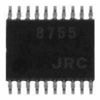
NJU8755V-TE1# NJR, NJU8755V-TE1# Datasheet

NJU8755V-TE1#
Specifications of NJU8755V-TE1#
NJU#8755V-TE1TR
NJU#8755V-TE1TR
NJU8755V-TE1#TR
Related parts for NJU8755V-TE1#
NJU8755V-TE1# Summary of contents
Page 1
... Built-in Low Voltage Detector Operating Voltage 2.7 to 5.25V CMOS Technology Package Outline SSOP20 BLOCK DIAGRAM IN L COM IN R Soft Start Ver.2008-11-19 TEST MUTE OUT OUT Low Voltage Control Logic MUTE STBY TEST NJU8755 PACKAGE OUTLINE NJU8755V PIN CONFIGURATION DDL SSL DDL DDL Pulse ...
Page 2
NJU8755 PIN DESCRIPTION No. SYMBOL TEST 4 MUTE DDL 10 6 OUT SSL 8 OUT DDR 16 13 OUT SSR ...
Page 3
FUNCTIONAL DESCRIPTION (1) Signal Output The OUT and OUT LP/LN RP/RN be converted to analog signal via external 2nd-order or higher LC filter. A switching regulator with a high response against a voltage fluctuation is the best selection for the ...
Page 4
NJU8755 ABSOLUTE MAXIMUM RATINGS PARAMETER Supply Voltage Input Voltage Operating Temperature Storage Temperature Power Dissipation Note 1) All voltage are relative to “V Note 2) The LSI must be used inside of the “Absolute maximum ratings”. Otherwise, a stress may ...
Page 5
ELECTRICAL CHARACTERISTICS PARAMETER Supply Voltage DD DDP DDN Input Impedance Voltage Gain Output Power Efficiency Output THD Output Power S/N Dynamic Range Channel Separation Output Level Difference Between L- and R- channels Maximum Mute Attenuation Operating Current ...
Page 6
NJU8755 TYPICAL APPLICATION CIRCUIT <LCR Filter Configuration> 0.1µF 10µ 2.2µ 10µF 2.2µ Figure 2.1. Application Circuit example <LR Filter Configuration> 0.1µF 10µ 2.2µ 10µF 2.2µ Figure 2.2. Application ...
Page 7
Using the LCR filter the power consumption is somewhat lower than using the LR filter power consumption when no signal input. The THD+N is somewhat influenced by the LR filter more than the LCR filter. Please test the circuit carefully ...


