AS1705V austriamicrosystems, AS1705V Datasheet - Page 13

AS1705V
Manufacturer Part Number
AS1705V
Description
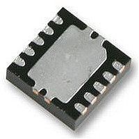
IC AMP AUDIO MONO 1.8W 10-DFN
Manufacturer
austriamicrosystems
Type
Class ABr
Datasheet
1.AS1702.pdf
(20 pages)
Specifications of AS1705V
Output Type
1-Channel (Mono)
Max Output Power X Channels @ Load
1.8W x 1 @ 4 Ohm
Voltage - Supply
2.7 V ~ 5.5 V
Features
Depop, Differential Inputs, Short-Circuit and Thermal Protection, Shutdown
Mounting Type
Surface Mount
Package / Case
10-TDFN Exposed Pad
No. Of Channels
1
Output Power
1.8W
Supply Voltage Range
2.7V To 5.5V
Load Impedance
4ohm
Operating Temperature Range
-40°C To +85°C
Amplifier Case Style
DFN
No. Of Pins
10
Rohs Compliant
Yes
Lead Free Status / RoHS Status
Lead free / RoHS Compliant
AS1702 - AS1705
Data Sheet
BTL Amplifier
All devices are designed to drive loads differentially in a bridge-tied load (BTL) configuration.
Figure 32. Bridge Tied Load Configuration
The BTL configuration doubles the output voltage (illustrated in
similar conditions. Thus, the differential gain of the device (A
effective gain is given by:
Substituting 2 x V
the output voltage:
Since the BTL outputs are biased at mid-supply, there is no net DC voltage across the load. This eliminates the need
for the large, expensive, performance degrading DC-blocking capacitors required by single-ended amplifiers.
Power Dissipation and Heat Sinking
Normally, the devices dissipate a significant amount of power. The maximum power dissipation is given in
Continuous Power Dissipation, or it can be calculated by:
where T
tor in ºC/W as specified in
The increased power delivered by a BTL configuration results in an increase in internal power dissipation versus a sin-
gle-ended configuration. The maximum internal power dissipation for a given V
www.austriamicrosystems.com
J(MAX)
- A p p l i c a t i o n I n f o r m a t i o n
is +150ºC, T
OUT(P-P)
for V
Table
AMB
OUT(P-P)
(see
3. For example, Θ
Table
into (EQ 3) and (EQ 4) yields four times the output power due to doubling of
3) is the ambient temperature, and Θ
P
P
DISSPKF(MAX)
DISSPKF(MAX)
V
A
JA
RMS
P
+1
-1
VD
OUT
Revision 1.47
of the TQFN package is +59.2ºC/W.
= 2 x
=
=
V
=
=
OUT(P-P)
VD
V
2 2
RMS
R
R
2V
T
π
) is twice the closed-loop gain of the input amplifier. The
R
L
Figure
IN
J(MAX)
2
F
CC
R
Θ
2
L
JA
2
-T
32) compared to a single-ended amplifier under
A
CC
JA
V
2 x V
V
OUT(P-P)
OUT(P-P)
and load is given by:
is the reciprocal of the derating fac-
OUT(P-P)
Table 3
(EQ 2)
(EQ 3)
(EQ 4)
(EQ 5)
(EQ 6)
13 - 20
as


