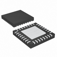
MAX9776ETJ+ Maxim Integrated Products, MAX9776ETJ+ Datasheet - Page 27

MAX9776ETJ+
Manufacturer Part Number
MAX9776ETJ+
Description
IC AMP AUDIO PWR 1.5W D 32TQFN
Manufacturer
Maxim Integrated Products
Series
DirectDrive™r
Type
Class Dr
Datasheet
1.MAX9776ETJ.pdf
(38 pages)
Specifications of MAX9776ETJ+
Output Type
1-Channel (Mono) with Stereo Headphones
Max Output Power X Channels @ Load
1.5W x 1 @ 4 Ohm; 60mW x 2 @ 16 Ohm
Voltage - Supply
2.7 V ~ 5.5 V
Features
Depop, Differential Inputs, I²C, Mute, Short-Circuit and Thermal Protection, Shutdown, Volume Control
Mounting Type
Surface Mount
Package / Case
32-TQFN Exposed Pad
Product
Class-D
Output Power
1.5 W
Common Mode Rejection Ratio (min)
45 dB
Thd Plus Noise
0.04 %
Operating Supply Voltage
2.7 V to 5.5 V
Supply Current
9.5 mA
Maximum Power Dissipation
1360 mW
Maximum Operating Temperature
+ 85 C
Mounting Style
SMD/SMT
Minimum Operating Temperature
- 40 C
Supply Voltage (max)
5.5 V
Supply Voltage (min)
2.7 V
Amplifier Class
D
No. Of Channels
3
Supply Voltage Range
2.7V To 5.5V
Load Impedance
4ohm
Operating Temperature Range
-40°C To +85°C
Amplifier Case Style
TQFN
Rohs Compliant
Yes
For Use With
MAX9776EVKIT+ - EVALUATION KIT FOR MAX9776
Lead Free Status / RoHS Status
Lead free / RoHS Compliant
A write to the MAX9775/MAX9776 includes transmis-
sion of a START condition, the slave address with the
R/W bit set to 0 (Table 1), one byte of data to configure
the Command Register, and a STOP condition. Figure
11 illustrates the proper format for one frame.
Figure 11. Write Data Format Example
Table 2. Control Registers
Table 3. Power-On Reset Conditions
Input Mode Control
Mono Volume Control
Left Volume Control
Right Volume Control
Output Mode Control
Global Control Register
Input Mode (000)
Mono Volume (001)
Left Volume (010)
Right Volume (011)
Output Mode (100)
Global Control Register (101)
COMMAND BYTE IS STORED ON
S
RECEIPT OF STOP CONDITION
SLAVE ADDRESS
FUNCTION
ACKNOWLEDGE FROM
MAX9775/MAX9776
COMMAND
2 x 1.5W, Stereo Class D Audio Subsystem
______________________________________________________________________________________
R/W
0
with DirectDrive Headphone Amplifier
ACK
FROM MAX9775/MAX9776
B7 B6 B5 B4 B3 B2
COMMAND BYTE
B7
0
0
0
0
1
1
COMMAND
ACKNOWLEDGE
Write Data Format
DATA
10000
11111
11111
11111
01000
00011
B6
0
0
1
1
0
0
B1 B0
ACK
B5
0
1
0
1
0
1
Input A gain = +20dB; input A, B, and C singled-ended stereo inputs
Maximum volume
Maximum volume
Maximum volume
0dB of extra mono gain, mode 8: stereo headphone, stereo speaker
Powered-off, input B/C gain = 0dB, MUTE off, SSM on, 3D/MONO on
P
MONO+6dB
INA+20dB
SHDN
B4
The MAX9775/MAX9776 only accept write data, but
they acknowledge the receipt of the address byte with
the R/W bit set high. The MAX9775/MAX9776 do not
write to the SDA bus in the event that the R/W bit is set
high. Subsequently, the master reads all 1’s from the
MAX9775/MAX9776. Always set the R/W bit to zero to
avoid this situation.
The MAX9775/MAX9776 are programmed through 6
control registers. Each register is addressed by the 3
MSBs (B5–B7) followed by 5 configure bits (B0–B4) as
shown in Table 2. Correct programming of the
MAX9775/MAX9776 requires writing to all 6 control reg-
isters. Upon power-on, their default settings are as list-
ed in Table 3.
Programming the MAX9775/MAX9776
IN+6dB
B3
DESCRIPTION
MVOL (Table 7)
RVOL (Table 7)
LVOL (Table 7)
INMODE (Tables 5a and 5b)
MUTE
B2
DATA
OUTMODE (Table 9)
SSM
B1
3D/MONO
B0
27


