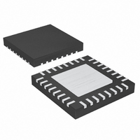
MAX9776ETJ+ Maxim Integrated Products, MAX9776ETJ+ Datasheet - Page 6

MAX9776ETJ+
Manufacturer Part Number
MAX9776ETJ+
Description
IC AMP AUDIO PWR 1.5W D 32TQFN
Manufacturer
Maxim Integrated Products
Series
DirectDrive™r
Type
Class Dr
Datasheet
1.MAX9776ETJ.pdf
(38 pages)
Specifications of MAX9776ETJ+
Output Type
1-Channel (Mono) with Stereo Headphones
Max Output Power X Channels @ Load
1.5W x 1 @ 4 Ohm; 60mW x 2 @ 16 Ohm
Voltage - Supply
2.7 V ~ 5.5 V
Features
Depop, Differential Inputs, I²C, Mute, Short-Circuit and Thermal Protection, Shutdown, Volume Control
Mounting Type
Surface Mount
Package / Case
32-TQFN Exposed Pad
Product
Class-D
Output Power
1.5 W
Common Mode Rejection Ratio (min)
45 dB
Thd Plus Noise
0.04 %
Operating Supply Voltage
2.7 V to 5.5 V
Supply Current
9.5 mA
Maximum Power Dissipation
1360 mW
Maximum Operating Temperature
+ 85 C
Mounting Style
SMD/SMT
Minimum Operating Temperature
- 40 C
Supply Voltage (max)
5.5 V
Supply Voltage (min)
2.7 V
Amplifier Class
D
No. Of Channels
3
Supply Voltage Range
2.7V To 5.5V
Load Impedance
4ohm
Operating Temperature Range
-40°C To +85°C
Amplifier Case Style
TQFN
Rohs Compliant
Yes
For Use With
MAX9776EVKIT+ - EVALUATION KIT FOR MAX9776
Lead Free Status / RoHS Status
Lead free / RoHS Compliant
2 x 1.5W, Stereo Class D Audio Subsystem
with DirectDrive Headphone Amplifier
ELECTRICAL CHARACTERISTICS (continued)
(V
0dB, volume setting = 0dB, mono path gain = 0dB, SHDN = 1, SSM = 1). Speaker load resistors (R
OUT_+ and OUT_-, headphone load resistors are terminated to GND, unless otherwise noted. C1 = C2 = C3 = 1µF. T
T
6
Note 1: All devices are 100% production tested at room temperature. All temperature limits are guaranteed by design.
Note 2: Measured at headphone outputs.
Note 3: Amplifier inputs AC-coupled to GND.
Note 4: Testing performed with a resistive load in series with an inductor to simulate an actual speaker load. For R
Note 5: MAX9775 only.
Note 6: Testing performed at room temperature with an 8Ω resistive load in series with a 68µH inductive load connected across BTL
Note 7: Guaranteed by design.
SDA, SCL Input Capacitance
Input Leakage Current
Pulse Width of Spike Suppressed
DIGITAL OUTPUTS (SDA Open Drain)
Output Low Voltage SDA
Output Fall Time SDA
I
Serial Clock Frequency
Bus Free Time Between STOP
and START Conditions
START Condition Hold
STOP Condition Setup Time
Clock Low Period
Clock High Period
Data Setup Time
Data Hold Time
Maximum Receive SCL/SDA Rise
Time
Maximum Receive SCL/SDA Fall
Time
Setup Time for STOP Condition
Capacitive Load for Each Bus
Line
MAX
2
DD
C INTERFACE TIMING (Note 7)
_______________________________________________________________________________________
, unless otherwise noted. Typical values are at T
= PV
for R
outputs for speaker amplifier. Testing performed with a 32Ω resistive load connected between OUT_ and GND for head-
phone amplifier. Testing performed with 32Ω resistive load connected between OUTRx and GND for mono receiver amplifi-
er. Mode transitions are controlled by I
DD
PARAMETER
L
= CPV
= 4Ω, L = 47µH.
DD
= 3.3V, V
GND
SYMBOL
= V
t
t
t
t
t
HD:DAT
HD:STA
SU:DAT
SU:STO
SU:STA
t
t
t
f
HIGH
V
LOW
C
t
BUF
t
SCL
C
I
PGND
SP
OF
t
t
IN
OL
R
F
IN
b
= V
2
C.
I
V
10pF to 400pF, I
SINK
CPGND
H(MIN)
A
= +25°C.) (Note 1)
= 6mA
to V
= 0V, SHDN = V
L(MAX)
CONDITIONS
SINK
bus capacitance =
= 3mA
DD
, I
2
C settings (INA gain = +20dB, INB gain = INC gain =
MIN
100
DC
1.3
0.6
0.6
1.3
0.6
0.6
0
LSP
TYP
250
0.3
10
50
) are terminated between
L
MAX
400
900
300
300
400
5.0
0.4
= 8Ω, L = 68µH;
A
= T
UNITS
kHz
pF
µA
pF
ns
ns
µs
µs
µs
µs
µs
ns
ns
ns
ns
µs
MIN
V
to


