AD8013AN Analog Devices Inc, AD8013AN Datasheet - Page 12
AD8013AN
Manufacturer Part Number
AD8013AN
Description
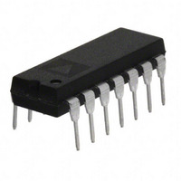
IC SINGLE SUPPLY OPAMP 14 DIP
Manufacturer
Analog Devices Inc
Datasheet
1.AD8013ARZ-14.pdf
(12 pages)
Specifications of AD8013AN
Rohs Status
RoHS non-compliant
Applications
Current Feedback
Number Of Circuits
3
-3db Bandwidth
140MHz
Slew Rate
1000 V/µs
Current - Supply
3.5mA
Current - Output / Channel
30mA
Voltage - Supply, Single/dual (±)
4.2 V ~ 13 V, ±2.1 V ~ 6.5 V
Mounting Type
Through Hole
Package / Case
14-DIP (0.300", 7.62mm)
Available stocks
Company
Part Number
Manufacturer
Quantity
Price


AD8013
2:1 Video Multiplexer
Configuring two amplifiers as unity gain followers and using the
third to set the gain results in a high performance 2:1 mux
(Figures 39 and 40). This circuit takes advantage of the very low
crosstalk between Channels 2 and 3 to achieve the OFF channel
isolation shown in Figure 40. This circuit can achieve
differential gain and phase of 0.03% and 0.07 respectively.
Figure 40. 2:1 Mux ON Channel Gain and Mux OFF Channel
Feedthrough vs. Frequency
Gain Switching
V
V
Figure 39. 2:1 Mux with High Isolation and Low
Differential Gain and Phase Errors
IN
IN
0.210 (5.33)
0.160 (4.06)
0.115 (2.93)
B
A
–1
–2
–3
–4
–5
–6
–7
–8
2
1
0
MAX
1M
0.022 (0.558)
0.014 (0.356)
13
12
10
9
14
1
2
3
PIN 1
2
3
14-Lead Plastic DIP (N-14)
0.795 (20.19)
0.725 (18.42)
DISABLE
DISABLE
14
8
0.100
(2.54)
BSC
10M
FREQUENCY – Hz
FEEDTHROUGH
0.070 (1.77)
0.045 (1.15)
R1
2k
R3
10
R4
10
R2
2k
8
7
0.060 (1.52)
0.015 (0.38)
0.280 (7.11)
0.240 (6.10)
SEATING
PLANE
0.130
(3.30)
MIN
100M
R6
845
6
5
GAIN
1
0.325 (8.25)
0.300 (7.62)
845
R5
0.015 (0.381)
0.008 (0.204)
7
Dimensions shown in inches and (mm).
0.195 (4.95)
0.115 (2.93)
1G
OUTLINE DIMENSIONS
–30
–40
–50
–60
–70
–80
V
OUT
–12–
The AD8013 can be used to build a circuit for switching between
any two arbitrary gains while maintaining a constant input
impedance. The example of Figure 41 shows a circuit for switching
between a noninverting gain of 1 and an inverting gain of 1. The
total time for channel switching and output voltage settling is
about 80 ns.
Figure 42. Switching Characteristic for Circuit of Figure 41
Figure 41. Circuit to Switch Between Gains of –1 and +1
0.1574 (4.00)
0.1497 (3.80)
0.0098 (0.25)
0.0040 (0.10)
V
SEATING
IN
PLANE
50
100
100
0%
90
10
0.0500
(1.27)
14
BSC
1
13
12
PIN 1
500mV
0.3444 (8.75)
0.3367 (8.55)
5V
14-Lead SOIC (R-14)
2k
0.0192 (0.49)
0.0138 (0.35)
14
500mV
1k
1k
0.0688 (1.75)
0.0532 (1.35)
8
7
698
845
0.2440 (6.20)
0.2284 (5.80)
0.0098 (0.25)
0.0075 (0.19)
10
6
5
9
698
845
DIS 3
+5V
DIS 1
–5V
11
4
1
3
7
8
200ns
8
0
0.0196 (0.50)
0.0099 (0.25)
15
0.0500 (1.27)
0.0160 (0.41)
V
OUT
x 45
REV. A
Related parts for AD8013AN
Image
Part Number
Description
Manufacturer
Datasheet
Request
R

Part Number:
Description:
AD8013-AR-14-EBZ-A01140-EB-014-3Z
Manufacturer:
Analog Devices Inc

Part Number:
Description:
±1.7g Dual-Axis IMEMS Accelerometer Evaluation Board
Manufacturer:
Analog Devices Inc
Datasheet:
Part Number:
Description:
Inertial Sensor Evaluation System
Manufacturer:
Analog Devices Inc
Datasheet:
Part Number:
Description:
Manufacturer:
Analog Devices Inc
Datasheet:
Part Number:
Description:
Manufacturer:
Analog Devices Inc
Datasheet:
Part Number:
Description:
Manufacturer:
Analog Devices Inc
Datasheet:
Part Number:
Description:
Manufacturer:
Analog Devices Inc
Datasheet:
Part Number:
Description:
Manufacturer:
Analog Devices Inc
Datasheet:
Part Number:
Description:
Manufacturer:
Analog Devices Inc
Datasheet:
Part Number:
Description:
Manufacturer:
Analog Devices Inc
Datasheet:
Part Number:
Description:
Manufacturer:
Analog Devices Inc
Datasheet:
Part Number:
Description:
Manufacturer:
Analog Devices Inc
Datasheet:
Part Number:
Description:
Manufacturer:
Analog Devices Inc
Datasheet: