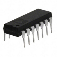
AD8013AN Analog Devices Inc, AD8013AN Datasheet - Page 9

AD8013AN
Manufacturer Part Number
AD8013AN
Description
IC SINGLE SUPPLY OPAMP 14 DIP
Manufacturer
Analog Devices Inc
Datasheet
1.AD8013ARZ-14.pdf
(12 pages)
Specifications of AD8013AN
Rohs Status
RoHS non-compliant
Applications
Current Feedback
Number Of Circuits
3
-3db Bandwidth
140MHz
Slew Rate
1000 V/µs
Current - Supply
3.5mA
Current - Output / Channel
30mA
Voltage - Supply, Single/dual (±)
4.2 V ~ 13 V, ±2.1 V ~ 6.5 V
Mounting Type
Through Hole
Package / Case
14-DIP (0.300", 7.62mm)
Available stocks
Company
Part Number
Manufacturer
Quantity
Price
REV. A
General
The AD8013 is a wide bandwidth, triple video amplifier that
offers a high level of performance on less than 4.0 mA per
amplifier of quiescent supply current. The AD8013 uses a
proprietary enhancement of a conventional current feedback
architecture, and achieves bandwidth in excess of 200 MHz with
low differential gain and phase errors, making it an extremely
efficient video amplifier.
The AD8013’s wide phase margin coupled with a high output
short circuit current make it an excellent choice when driving
any capacitive load. High open-loop gain and low inverting
input bias current enable it to be used with large values of
feedback resistor with very low closed-loop gain errors.
It is designed to offer outstanding functionality and performance
at closed-loop inverting or noninverting gains of one or greater.
Choice of Feedback & Gain Resistors
Because it is a current feedback amplifier, the closed-loop band-
width of the AD8013 may be customized using different values
of the feedback resistor. Table I shows typical bandwidths at
different supply voltages for some useful closed-loop gains when
driving a load of 150 .
The choice of feedback resistor is not critical unless it is
important to maintain the widest, flattest frequency response.
The resistors recommended in the table are those (chip
resistors) that will result in the widest 0.1 dB bandwidth without
peaking. In applications requiring the best control of bandwidth,
1% resistors are adequate. Package parasitics vary between the
14-pin plastic DIP and the 14-pin plastic SOIC, and may result
in a slight difference in the value of the feedback resistor used to
achieve the optimum dynamic performance. Resistor values and
widest bandwidth figures are shown in parenthesis for the SOIC
where they differ from those of the DIP. Wider bandwidths than
those in the table can be attained by reducing the magnitude of
the feedback resistor (at the expense of increased peaking),
while peaking can be reduced by increasing the magnitude of
the feedback resistor.
Increasing the feedback resistor is especially useful when driving
large capacitive loads as it will increase the phase margin of the
closed-loop circuit. (Refer to the section on driving capacitive
loads for more information.)
Figure 27. Closed-Loop Gain and Phase vs. Frequency,
G = –10, R
+1
–1
–2
–3
–4
–5
–6
0
1M
L
PHASE
= 150
GAIN
10M
FREQUENCY – Hz
V
S
V
= +5V
S
= +5V
100M
V
S
V
= 5V
S
G = –10
R
= 5V
L
= 150
1G
90
0
180
–90
–9–
To estimate the –3 dB bandwidth for closed-loop gains of 2 or
greater, for feedback resistors not listed in the following table,
the following single pole model for the AD8013 may be used:
where:
The –3 dB bandwidth is determined from this model as:
This model will predict –3 dB bandwidth to within about 10%
to 15% of the correct value when the load is 150
bandwidth. The model is not accurate enough to predict either
the phase behavior or the frequency response peaking of the
AD8013.
It should be noted that the bandwidth is affected by attenuation
due to the finite input resistance. Also, the open-loop output
resistance of about 12
driving load resistors less than about 250 . (Bandwidths will
be about 10% greater for load resistances above a few hundred
ohms.)
Table I. –3 dB Bandwidth vs. Closed-Loop Gain and Feedback
Resistor, R
V
+5
Driving Capacitive Loads
When used in combination with the appropriate feedback
resistor, the AD8013 will drive any load capacitance without
oscillation. The general rule for current feedback amplifiers is
that the higher the load capacitance, the higher the feedback
resistor required for stable operation. Due to the high open-loop
transresistance and low inverting input current of the AD8013,
the use of a large feedback resistor does not result in large closed-
loop gain errors. Additionally, its high output short circuit current
makes possible rapid voltage slewing on large load capacitors.
For the best combination of wide bandwidth and clean pulse
response, a small output series resistor is also recommended.
Table II contains values of feedback and series resistors which
result in the best pulse responses. Figure 29 shows the AD8013
driving a 300 pF capacitor through a large voltage step with
virtually no overshoot. (In this case, the large and small signal
pulse responses are quite similar in appearance.)
5 V. For lower supply voltages there will be a slight decrease in
5
S
– Volts
C
R
G = ideal closed loop gain
Gn = 1
rin = inverting input resistance
ACL = closed loop gain
L
T
F
= 150
= feedback resistor
= transcapacitance
ACL
Gain
+1
+2
+10
–1
–10
+1
+2
+10
–1
–10
f
3
(SOIC)
R
R
G
F
2
reduces the bandwidth somewhat when
1 SC
= noise gain
C
T
(R
R
2000
845 (931)
301
698 (825)
499
2000
887 (931)
301
698 (825)
499
T
F
F
1
(R
– Ohms
1 pF
G
F
Gn rin )
Gn rin )
150
AD8013
BW – MHz
230
150 (135)
80
140 (130)
85
180
120 (130)
75
130 (120)
80
and V
S
=


