AD532SH Analog Devices Inc, AD532SH Datasheet - Page 2
AD532SH
Manufacturer Part Number
AD532SH
Description
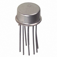
IC MULTIPLIER 10V TO-100-10
Manufacturer
Analog Devices Inc
Specifications of AD532SH
Package / Case
TO-100, Metal Can (10 Leads)
Rohs Status
RoHS non-compliant
Function
Analog Multiplier/Divider
Number Of Bits/stages
4-Quadrant
Termination Type
Through Hole
Mounting Type
Through Hole
No. Of Channels
4
Analog Multiplexer Type
Multiplier-Divider
Lead Free Status / RoHS Status
Available stocks
Company
Part Number
Manufacturer
Quantity
Price


AD532–SPECIFICATIONS
Model
MULTIPLIER PERFORMANCE
DYNAMICS
NOISE
OUTPUT
INPUT AMPLIFIERS (X, Y, and Z)
DIVIDER PERFORMANCE
SQUARE PERFORMANCE
SQUARE ROOTER PERFORMANCE
POWER SUPPLY SPECIFICATIONS
PACKAGE OPTIONS
Specifications subject to change without notice.
Specifications shown in boldface are tested on all production units at final
electrical test. Results from those tests are used to calculate outgoing quality
levels. All min and max specifications are guaranteed, although only those shown
in boldface are tested on all production units.
Transfer Function
Total Error (–10 V ≤ X, Y ≤ +10 V)
T
Total Error vs. Temperature
Supply Rejection (± 15 V ± 10%)
Nonlinearity, X (X = 20 V p-p, Y = 10 V)
Nonlinearity, Y (Y = 20 V p-p, X = 10 V)
Feedthrough, X (Y Nulled,
Feedthrough, Y (X Nulled,
Feedthrough vs. Temperature
Feedthrough vs. Power Supply
Small Signal BW (V
1% Amplitude Error
Slew Rate (V
Settling Time (to 2%, ∆V
Wideband Noise f = 5 Hz to 10 kHz
Wideband Noise
Output Voltage Swing
Output Impedance (f ≤ 1 kHz)
Output Offset Voltage
Output Offset Voltage vs. Temperature
Output Offset Voltage vs. Supply
Signal Voltage Range (Diff. or CM
CMRR
Input Bias Current
Offset Current
Differential Resistance
Transfer Function (X
Total Error
Transfer Function
Total Error
Transfer Function
Total Error (0 V ≤ V
Supply Voltage
Supply Current
TO-116 (D-14)
TO-100 (H-10A)
LCC (E-20A)
A
Operating Diff)
X, Y Inputs
X, Y Inputs T
Z Input
Z Input T
X = 20 V p-p 50 Hz)
Y = 20 V p-p 50 Hz)
(V
(V
Rated Performance
Operating
Quiescent
= Min to Max
X
X
= –10 V, –10 V ≤ V
= –1 V, –10 V ≤ V
MIN
OUT
MIN
to T
f = 5 Hz to 5 MHz
20 p-p)
OUT
to T
MAX
Z
l
≤ 10 V)
> X
= 0.1 rms)
MAX
Z
OUT
2
Z
≤ +10 V)
)
≤ +10 V)
= 20 V)
Min
± 10
40
± 10
AD532JD
AD532JH
(X
10 V
(X
1
10 V Z/(X
– X
1
– X
AD532J
2
(@ 25 C, V
)
Typ
10 V
± 1.5
± 2.5
± 0.04
± 0.05
± 0.8
± 0.3
50
30
2.0
± 0.25
1
75
45
1
0.6
3.0
± 13
1
± 40
0.7
± 2.5
± 10
3
10
± 10
± 30
± 0.3
10
± 2
± 4
± 0.8
–√10 V Z
± 1.5
± 15
4
2
2
)(Y
1
– X
1
– Y
2
)
2
Max
200
150
6
S
)
=
2.0
18
15 V, R ≥ 2 k
Min
± 10
50
± 10
AD532KD
AD532KH
THERMAL CHARACTERISTICS
H-10A: θ
E-20A: θ
D-14: θ
(X
10 V Z/(X
10 V
(X
1
– X
1
AD532K
– X
2
JC
)
Typ
10 V
± 0.7
± 1.5
± 0.03
± 0.05
± 0.5
± 0.2
30
25
1.0
± 0.25
1
75
45
1
0.6
3.0
± 13
1
0.7
± 2.5
± 10
1.5
8
± 5
± 25
± 0.1
10
± 1
± 3
± 0.4
–√10 V Z
± 1.0
± 15
4
2
2
JC
JC
)(Y
= 22°C/W; θ
1
= 22°C/W; θ
= 25°C/W; θ
– X
V
1
OS
– Y
2
grounded, unless otherwise noted.)
)
2
Max
100
80
4
6
)
1.0
30
15
18
JA
JA
JA
Min
± 10
50
± 10
AD532SD
AD532SH
AD532SE/883B
= 85°C/W
(X
= 85°C/W
= 150°C/W
(X
10 V
1
10 V Z/(X
– X
1
AD532S
– X
2
)
Typ
10 V
± 0.5
± 0.01
± 0.05
± 0.5
± 0.2
30
25
1.0
± 0.25
1
75
45
1
0.6
3.0
± 13
1
± 2.5
± 10
1.5
8
± 5
± 25
± 0.1
10
± 1
± 3
± 0.4
–√10 V Z
± 1.0
± 15
4
2
2
)(Y
1
1
– X
– Y
2
2
)
Max
100
80
2.0
4
± 22
6
)
1.0
4.0
0.04
30
15
Unit
%
%
%/°C
%/%
%
%
mV
mV
mV p-p/°C
mV/%
MHz
kHz
V/µs
µs
mV (rms)
mV (rms)
V
Ω
mV
mV/°C
mV/%
V
dB
µA
µA
µA
µA
µA
MΩ
%
%
%
%
V
V
mA
Related parts for AD532SH
Image
Part Number
Description
Manufacturer
Datasheet
Request
R

Part Number:
Description:
±1.7g Dual-Axis IMEMS Accelerometer Evaluation Board
Manufacturer:
Analog Devices Inc
Datasheet:

Part Number:
Description:
Inertial Sensor Evaluation System
Manufacturer:
Analog Devices Inc
Datasheet:
Part Number:
Description:
Manufacturer:
Analog Devices Inc
Datasheet:
Part Number:
Description:
Manufacturer:
Analog Devices Inc
Datasheet:
Part Number:
Description:
Manufacturer:
Analog Devices Inc
Datasheet:
Part Number:
Description:
Manufacturer:
Analog Devices Inc
Datasheet:
Part Number:
Description:
Manufacturer:
Analog Devices Inc
Datasheet:
Part Number:
Description:
Manufacturer:
Analog Devices Inc
Datasheet:
Part Number:
Description:
Manufacturer:
Analog Devices Inc
Datasheet:
Part Number:
Description:
Manufacturer:
Analog Devices Inc
Datasheet:
Part Number:
Description:
Manufacturer:
Analog Devices Inc
Datasheet:
Part Number:
Description:
Manufacturer:
Analog Devices Inc
Datasheet:
Part Number:
Description:
Manufacturer:
Analog Devices Inc
Datasheet: