AD532SH Analog Devices Inc, AD532SH Datasheet - Page 6
AD532SH
Manufacturer Part Number
AD532SH
Description
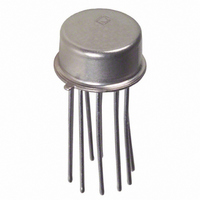
IC MULTIPLIER 10V TO-100-10
Manufacturer
Analog Devices Inc
Specifications of AD532SH
Package / Case
TO-100, Metal Can (10 Leads)
Rohs Status
RoHS non-compliant
Function
Analog Multiplier/Divider
Number Of Bits/stages
4-Quadrant
Termination Type
Through Hole
Mounting Type
Through Hole
No. Of Channels
4
Analog Multiplexer Type
Multiplier-Divider
Lead Free Status / RoHS Status
Available stocks
Company
Part Number
Manufacturer
Quantity
Price


APPLICATIONS CONSIDERATIONS
The performance and ease of use of the AD532 is achieved
through the laser trimming of thin-film resistors deposited
directly on the monolithic chip. This trimming-on-the-chip
technique provides a number of significant advantages in terms
of cost, reliability and flexibility over conventional in-package
trimming of off-the-chip resistors mounted or deposited on a
hybrid substrate.
First and foremost, trimming on the chip eliminates the need for
a hybrid substrate and the additional bonding wires that are
required between the resistors and the multiplier chip. By trim-
ming more appropriate resistors on the AD532 chip itself, the
second input terminals that were once committed to external
trimming networks have been freed to allow fully differential
operation at both the X and Y inputs. Further, the requirement
for an input attenuator to adjust the gain at the Y input has been
eliminated, letting the user take full advantage of the high input
impedance properties of the input differential amplifiers. Thus, the
AD532 offers greater flexibility for both algebraic computation and
transducer instrumentation applications.
Finally, provision for fine trimming the output voltage offset has
been included. This connection is optional, however, as the
AD532 has been factory-trimmed for total performance as
described in the listed specifications.
REPLACING OTHER IC MULTIPLIERS
Existing designs using IC multipliers that require external
trimming networks can be simplified using the pin-for-pin
replaceability of the AD532 by merely grounding the X
V
when unused.)
APPLICATIONS
MULTIPLICATION
For operation as a multiplier, the AD532 should be connected
as shown in Figure 11. The inputs can be fed differentially to
the X and Y inputs, or single-ended by simply grounding the
unused input. Connect the inputs according to the desired
polarity in the output. The Z terminal is tied to the output to
close the feedback loop around the op amp (see Figure 1). The
offset adjust V
zero volts to obtain zero out, or to buck out other system offsets.
AD532
OS
terminals. (The V
X
X
Y
Y
(OPTIONAL)
1
2
1
2
OS
is optional and is adjusted when both inputs are
+V
S
AD532
OS
20k
V
OS
terminal should always be grounded
–V
S
Z
OUT
V
OUT
=
(X
V
1
OUT
– X
2
10V
) (Y
1
– Y
2
)
2
, Y
2
and
SQUARE
The squaring circuit in Figure 12 is a simple variation of the
multiplier. The differential input capability of the AD532, how-
ever, can be used to obtain a positive or negative output response
to the input . . . a useful feature for control applications, as it
might eliminate the need for an additional inverter somewhere else.
DIVISION
The AD532 can be configured as a two-quadrant divider by
connecting the multiplier cell in the feedback loop of the op
amp and using the Z terminal as a signal input, as shown in
Figure 13. It should be noted, however, that the output error is
given approximately by 10 V
error specification for the multiply mode; and bandwidth by
f
Further, to avoid positive feedback, the X input is restricted to
negative values. Thus for single-ended negative inputs (0 V to
–10 V), connect the input to X and the offset null to X
single-ended positive inputs (0 V to +10 V), connect the input
to X
(S.F.) and offset (X
and explained in Table I.
For practical reasons, the useful range in denominator input is
approximately 500 mV ≤ |(X
adjust (V
full scale.
Adjust
Scale Factor –10 V
X
Repeat if required.
m
0
× (X
(Offset)
Table I. Adjust Procedure (Divider or Square Rooter)
2
and the offset null to X
1
– X
OS
2.2k
), if used, is trimmed with Z at zero and (X
2
)/10 V, where f
V
IN
With:
X
–1 V
Z
X
X
X
Y
Y
DIVIDER
0
2
2
1
1
47k
) adjustments are recommended as shown
+V
+V
S
Z
+10 V
+0.1 V –1 V
AD532
S
X
Y
X
Y
20k
V
1
2
1
2
OS
+V
+V
m
S
S
–V
AD532
1
–V
1
. For optimum performance, gain
is the bandwidth of the multiplier.
20k
m
– X
S
S
(X
Z
/(X
0
Adjust
for:
V
–10 V
OUT
)
(OPTIONAL)
2
OUT
–V
–V
1
)| ≤ 10 V. The voltage offset
– X
Z
S
S
OUT
2
), where
V
OUT
SQUARE ROOTER
With:
Z
+10 V
+0.1 V
V
V
OUT
OUT
= 10VZ
10k
1k
(SF)
=
V
X
10V
V
IN
OUT
2
m
is the total
1
– X
Adjust
for:
V
–10 V
–1 V
2
OUT
; for
2
) at
Related parts for AD532SH
Image
Part Number
Description
Manufacturer
Datasheet
Request
R

Part Number:
Description:
±1.7g Dual-Axis IMEMS Accelerometer Evaluation Board
Manufacturer:
Analog Devices Inc
Datasheet:

Part Number:
Description:
Inertial Sensor Evaluation System
Manufacturer:
Analog Devices Inc
Datasheet:
Part Number:
Description:
Manufacturer:
Analog Devices Inc
Datasheet:
Part Number:
Description:
Manufacturer:
Analog Devices Inc
Datasheet:
Part Number:
Description:
Manufacturer:
Analog Devices Inc
Datasheet:
Part Number:
Description:
Manufacturer:
Analog Devices Inc
Datasheet:
Part Number:
Description:
Manufacturer:
Analog Devices Inc
Datasheet:
Part Number:
Description:
Manufacturer:
Analog Devices Inc
Datasheet:
Part Number:
Description:
Manufacturer:
Analog Devices Inc
Datasheet:
Part Number:
Description:
Manufacturer:
Analog Devices Inc
Datasheet:
Part Number:
Description:
Manufacturer:
Analog Devices Inc
Datasheet:
Part Number:
Description:
Manufacturer:
Analog Devices Inc
Datasheet:
Part Number:
Description:
Manufacturer:
Analog Devices Inc
Datasheet: