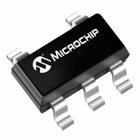
MCP6546UT-E/OT Microchip Technology, MCP6546UT-E/OT Datasheet - Page 14

MCP6546UT-E/OT
Manufacturer Part Number
MCP6546UT-E/OT
Description
IC COMP O-D 1.6V SNGL SOT23-5
Manufacturer
Microchip Technology
Type
General Purposer
Specifications of MCP6546UT-E/OT
Output Type
CMOS, Open-Drain, Rail-to-Rail, TTL
Package / Case
SC-74A, SOT-753
Number Of Elements
1
Voltage - Supply
1.6 V ~ 5.5 V
Mounting Type
Surface Mount
Number Of Channels
1 Channel
Response Time
4 us
Offset Voltage (max)
7 mV
Input Bias Current (max)
0.000001 uA
Supply Voltage (max)
5.5 V
Supply Voltage (min)
1.6 V
Maximum Operating Temperature
+ 125 C
Mounting Style
SMD/SMT
Minimum Operating Temperature
- 40 C
Comparator Type
Low Power
No. Of Comparators
1
Ic Output Type
Open Drain
Output Compatibility
CMOS, TTL
Supply Current
0.6µA
Supply Voltage Range
1.6V To 5.5V
Amplifier Case Style
SOT-23
Rohs Compliant
Yes
Lead Free Status / RoHS Status
Lead free / RoHS Compliant
Other names
MCP6546UT-E/OT
MCP6546UT-E/OTTR
MCP6546UT-E/OTTR
Available stocks
Company
Part Number
Manufacturer
Quantity
Price
Part Number:
MCP6546UT-E/OT
Manufacturer:
MICROCHI
Quantity:
20 000
MCP6546/6R/6U/7/8/9
4.0
The MCP6546/6R/6U/7/8/9 family of push-pull output
comparators are fabricated on Microchip’s state-of-the-
art CMOS process. They are suitable for a wide range
of applications requiring very low power consumption.
4.1
4.1.1
The MCP6546/6R/6U/7/8/9 comparator family uses
CMOS transistors at the input. They are designed to
prevent phase inversion when the input pins exceed
the supply voltages.
exceeding both supplies with no resulting phase
inversion.
4.1.2
The ESD protection on the inputs can be depicted as
shown in
tect the input transistors, and to minimize input bias
current (IB). The input ESD diodes clamp the inputs
when they try to go more than one diode drop below
V
above V
allow normal operation, and low enough to bypass ESD
events within the specified limits.
FIGURE 4-1:
Structures.
In order to prevent damage and/or improper operation
of these amplifiers, the circuits they are in must limit the
currents (and voltages) at the V
Absolute Maximum Ratings † at the beginning of
Section 1.0 “Electrical Characteristics”).
shows the recommended approach to protecting these
inputs. The internal ESD diodes prevent the input pins
(V
the resistors R
out of the input pin. Diodes D
pin (V
When implemented as shown, resistors R
limit the current through D
DS21714F-page 14
SS
IN
. They also clamp any voltages that go too far
+ and V
V
V
V
IN
IN
DD
SS
+
+ and V
DD
APPLICATIONS INFORMATION
Comparator Inputs
Figure
; their breakdown voltage is high enough to
Bond
Bond
Bond
PHASE REVERSAL
INPUT VOLTAGE AND CURRENT
LIMITS
Pad
Pad
Pad
IN
–) from going too far below ground, and
1
and R
4-1. This structure was chosen to pro-
IN
–) from going too far above V
Figure 2-3
2
Simplified Analog Input ESD
limit the possible current drawn
Stage
Input
1
and D
1
and D
shows an input voltage
IN
+ and V
2
.
2
Bond
prevent the input
Pad
1
IN
and R
– pins (see
Figure 4-3
V
IN
–
2
also
DD
.
FIGURE 4-2:
Inputs.
It is also possible to connect the diodes to the left of the
resistors R
the diodes D
mechanism. The resistor then serves as in-rush current
limiter; the DC current into the input pins (V
V
A significant amount of current can flow out of the
inputs when the common mode voltage (V
ground (V
high impedance may need to limit the useable voltage
range.
4.1.3
The input stage of this family of devices uses two
differential input stages in parallel: one operates at low
input voltages and the other at high input voltages.
With this topology, the input voltage is 0.3V above V
and 0.3V below V
measured at both V
proper operation.
The MCP6546/6R/6U/7/8/9 family has internally-set
hysteresis that is small enough to maintain input offset
accuracy (<7 mV), and large enough to eliminate
output chattering caused by the comparator’s own
input noise voltage (200 µV
this capability.
IN
–) should be very small.
V
V
1
2
R
R
SS
1
1
2
NORMAL OPERATION
and R
1
R
≥
≥
); see
R
and D
1
D
2
V
V
1
SS
SS
D
2
– (minimum expected V
– (minimum expected V
SS
. In this case, the currents through
2
Figure
2
SS
need to be limited by some other
- 0.3V and V
Protecting the Analog
. The input offset voltage is
© 2007 Microchip Technology Inc.
2-42. Applications that are
2 mA
MCP6G0X
2 mA
+
–
P-P
R
V
3
).
DD
Figure 4-3
DD
+ 0.3V to ensure
CM
1
2
)
V
)
) is below
illustrates
OUT
IN
+ and
DD


