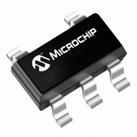
MCP6546UT-E/OT Microchip Technology, MCP6546UT-E/OT Datasheet - Page 2

MCP6546UT-E/OT
Manufacturer Part Number
MCP6546UT-E/OT
Description
IC COMP O-D 1.6V SNGL SOT23-5
Manufacturer
Microchip Technology
Type
General Purposer
Specifications of MCP6546UT-E/OT
Output Type
CMOS, Open-Drain, Rail-to-Rail, TTL
Package / Case
SC-74A, SOT-753
Number Of Elements
1
Voltage - Supply
1.6 V ~ 5.5 V
Mounting Type
Surface Mount
Number Of Channels
1 Channel
Response Time
4 us
Offset Voltage (max)
7 mV
Input Bias Current (max)
0.000001 uA
Supply Voltage (max)
5.5 V
Supply Voltage (min)
1.6 V
Maximum Operating Temperature
+ 125 C
Mounting Style
SMD/SMT
Minimum Operating Temperature
- 40 C
Comparator Type
Low Power
No. Of Comparators
1
Ic Output Type
Open Drain
Output Compatibility
CMOS, TTL
Supply Current
0.6µA
Supply Voltage Range
1.6V To 5.5V
Amplifier Case Style
SOT-23
Rohs Compliant
Yes
Lead Free Status / RoHS Status
Lead free / RoHS Compliant
Other names
MCP6546UT-E/OT
MCP6546UT-E/OTTR
MCP6546UT-E/OTTR
Available stocks
Company
Part Number
Manufacturer
Quantity
Price
Part Number:
MCP6546UT-E/OT
Manufacturer:
MICROCHI
Quantity:
20 000
MCP6546/6R/6U/7/8/9
1.0
Absolute Maximum Ratings †
V
Open-Drain output............................................... V
Analog Input (V
All other inputs and outputs ........... V
Difference Input voltage ...................................... |V
Output Short-Circuit Current .................................continuous
Current at Input Pins ....................................................±2 mA
Current at Output and Supply Pins ............................±30 mA
Storage temperature .....................................-65°C to +150°C
Maximum Junction Temperature (T
ESD protection on all pins:
DC CHARACTERISTICS
DS21714F-page 2
Electrical Specifications: Unless otherwise indicated, V
R
Power Supply
Supply Voltage
Quiescent Current
(per comparator)
Input
Input Voltage Range
Common Mode Rejection Ratio
Common Mode Rejection Ratio
Common Mode Rejection Ratio
Power Supply Rejection Ratio
Input Offset Voltage
Input Hysteresis Voltage
Input Bias Current
Input Offset Current
Common Mode Input Impedance
Differential Input Impedance
Note 1:
DD
(HBM;MM) .....................................2 kV;200V (MCP6546U)
(HBM;MM) ................................ 4 kV; 200V (all other parts)
PU
Drift with Temperature
Linear Temp. Co.
Quadratic Temp. Co.
At Temperature (I-Temp parts)
At Temperature (E-Temp parts)
- V
= 2.74 kΩ to V
SS
2:
3:
4:
ELECTRICAL
CHARACTERISTICS
.........................................................................7.0V
Parameters
The input offset voltage is the center of the input-referred trip points. The input hysteresis is the difference between the
input-referred trip points.
V
Input bias current at temperature is not tested for the SC-70-5 package
Do not short the output above V
V
HYST
PU
IN
+, V
test limit was V
at differential temperatures is estimated using: V
PU
IN
-)††............. V
= V
DD
(Refer to
DD
J
) .......................... +150°C
before Dec. 2004 (week code 52).
SS
ΔV
SS
CMRR
CMRR
CMRR
PSRR
V
Figure
V
Z
Sym
– 0.3V to V
V
V
OS
TC
TC
Z
- 1.0V to V
HYST
I
CMR
DIFF
I
OS
I
I
I
CM
DD
OS
Q
B
B
B
/ΔT
1
2
SS
A
1-3).
+ 10V. Limit the output current to Absolute Maximum Rating of 30 mA. The minimum
V
SS
SS
DD
DD
DD
Min
-7.0
1.6
0.3
1.5
55
50
55
63
—
—
—
—
—
—
—
—
—
+ 10.5V
− 0.3
+ 1.0V
+ 0.3V
– V
DD
SS
|
10
10
= +1.6V to +5.5V, V
-0.035
1200
Typ
±1.5
0.6
3.3
6.7
70
65
70
80
25
—
—
±3
±1
13
13
1
||4
||2
HYST
V
† Notice: Stresses above those listed under “Absolute Maxi-
mum Ratings” may cause permanent damage to the device.
This is a stress rating only and functional operation of the
device at those or any other conditions above those indicated
in the operational listings of this specification is not implied.
Exposure to maximum rating conditions for extended periods
may affect device reliability.
†† See Section 4.1.2 “Input Voltage and Current
Limits”
DD
Max
5000
+7.0
100
5.5
6.5
—
—
—
—
—
—
—
—
—
—
—
(T
1
+ 0.3
A
) = V
SS
µV/°C
Units
HYST
µV/°C T
µV/°C T
Ω||pF
Ω||pF
mV
mV
µA
dB
dB
dB
dB
pA
pA
pA
pA
= GND, T
V
V
+ (T
2
V
I
V
V
V
V
V
V
T
V
T
T
V
OUT
A
A
A
A
A
PU
DD
DD
DD
CM
CM
CM
CM
CM
A
= -40°C to +125°C, V
= -40°C to +125°C, V
= -40°C to +125°C, V
= +85°C, V
= +125°C, V
-25°C) TC
A
≥ V
= 5V, V
= 5V, V
= 5V, V
= V
= V
= V
= V
= V
= 0
= 25°C, V
DD
SS
SS
SS
SS
SS
© 2007 Microchip Technology Inc.
(Note 1)
(Note 1)
CM
CM
CM
1
CM
Conditions
IN
CM
+ (T
= -0.3V to 5.3V
= 2.5V to 5.3V
= -0.3V to 2.5V
+ = V
= V
= V
A
SS
- 25°C)
SS
DD
(Note 3)
CM
CM
CM
/2, V
(Note 3)
= V
= V
= V
2
TC
IN
SS
SS
SS
– = V
2
.
(Note 2)
(Note 2)
SS
,


