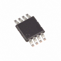
MAX921CUA+ Maxim Integrated Products, MAX921CUA+ Datasheet - Page 10

MAX921CUA+
Manufacturer Part Number
MAX921CUA+
Description
IC COMPARATOR W/REF 8-UMAX
Manufacturer
Maxim Integrated Products
Type
with Voltage Referencer
Datasheet
1.MAX922CSA.pdf
(17 pages)
Specifications of MAX921CUA+
Number Of Elements
1
Output Type
CMOS, TTL
Voltage - Supply
2.5 V ~ 11 V, ±1.25 V ~ 5.5 V
Mounting Type
Surface Mount
Package / Case
8-TSSOP, 8-MSOP (0.118", 3.00mm Width)
Number Of Channels
1 Channel
Product
Analog Comparators
Offset Voltage (max)
+/- 10 mV
Supply Voltage (max)
11 V
Supply Voltage (min)
2.5 V
Supply Current (max)
3.2 uA
Maximum Power Dissipation
330 mW
Maximum Operating Temperature
+ 70 C
Mounting Style
SMD/SMT
Minimum Operating Temperature
0 C
Comparator Type
General Purpose
No. Of Comparators
1
Response Time
12µs
Ic Output Type
CMOS, TTL
Supply Current
2.5µA
Supply Voltage Range
± 1.25V To ± 5.5V
Amplifier Case Style
µMAX
Rohs Compliant
Yes
Lead Free Status / RoHS Status
Lead free / RoHS Compliant
comparator is used with the reference, the combined
peak-to-peak noise is about 1mV. This, of course, is
much higher than the RMS noise of the individual
components. Care should be taken in the layout to
avoid capacitive coupling from any output to the
reference pin. Crosstalk can significantly increase the
actual noise of the reference.
Hysteresis increases the comparators’ noise margin by
increasing the upper threshold and decreasing the
lower threshold (see Figure 2).
To add hysteresis to the MAX921 or MAX923, connect
resistor R1 between REF and HYST, and connect
resistor R2 between HYST and V- (Figure 3). If no
hysteresis is required, connect HYST to REF. When
hysteresis is added, the upper threshold increases by
the same amount that the lower threshold decreases.
The hysteresis band (the difference between the upper
and lower thresholds, V
twice the voltage between REF and HYST. The HYST
input can be adjusted to a maximum voltage of REF
and to a minimum voltage of (REF – 50mV). The
maximum difference between REF and HYST (50mV)
will therefore produce a 100mV max hysteresis band.
Use the following equations to determine R1 and R2:
Where I
should not exceed the REF source capability, and
should be significantly larger than the HYST input
current. I
usually appropriate. If 2.4MΩ is chosen for R2 (I
0.5µA), the equation for R1 and V
approximated as:
When hysteresis is obtained in this manner for the
MAX923, the same hysteresis applies to both comparators.
Hysteresis can be set with two resistors using positive
feedback, as shown in Figure 4. This circuit generally
draws more current than the circuits using the HYST
pin on the MAX921 and MAX923, and the high
Ultra Low-Power,
Single/Dual-Supply Comparators
10
__________Applications Information
R1 (k ) = V
R1 =
R2 =
______________________________________________________________________________________
Ω
REF
(
⎛
⎜
⎝
2
1.182 –
REF
×
V
(the current sourced by the reference)
HB
HB
I
I
REF
values between 0.1µA and 4µA are
REF
(mV)
)
V
HB
2
Hysteresis (MAX921/MAX923)
Hysteresis (MAX922/MAX924)
⎞
⎟
⎠
HB
) is approximately equal to
Hysteresis
HB
can be
REF
=
feedback impedance slows hysteresis. The design
procedure is as follows:
Figure 4. External Hysteresis
1. Choose R3. The leakage current of IN+ is under
2. Choose the hysteresis voltage (V
3. Calculate R1.
4. Choose the threshold voltage for V
5. Calculate R2.
1nA (up to +85°C), so the current through R3 can be
around 100nA and still maintain good accuracy.
The current through R3 at the trip point is V
or 100nA for R3 = 11.8MΩ. 10MΩ is a good
practical value.
between the upper and lower thresholds. In this
example, choose V
R1 = R3
In this example, choose V
A 1% preferred value is 64.9kΩ.
R2 =
V
IN
=
=
=
=
10M
100k
65.44k
⎡
⎢
⎢
⎣
⎡
⎢
⎢
⎣
⎛
⎜
⎝
⎛
⎜
⎝
R1
(V
(1.182
×
Ω
×
REF
Ω
V
V
R2
V
0.05
THR
HB
5
+
×
3
×
R1)
HB
100k)
1
V
REF
⎞
⎟ −
⎠
= 50mV.
1
R1
⎞
⎟ −
⎠
1
R3
MAX924
THR
GND
−
100k
= 3V.
R3
1
1
V+
V+
⎤
⎥
⎥
⎦
V-
−
HB
10M
IN
OUT
1
), the voltage
rising (V
⎤
⎥
⎥
⎦
REF
THR
/R3,
).


