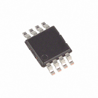
MAX921CUA+ Maxim Integrated Products, MAX921CUA+ Datasheet - Page 11

MAX921CUA+
Manufacturer Part Number
MAX921CUA+
Description
IC COMPARATOR W/REF 8-UMAX
Manufacturer
Maxim Integrated Products
Type
with Voltage Referencer
Datasheet
1.MAX922CSA.pdf
(17 pages)
Specifications of MAX921CUA+
Number Of Elements
1
Output Type
CMOS, TTL
Voltage - Supply
2.5 V ~ 11 V, ±1.25 V ~ 5.5 V
Mounting Type
Surface Mount
Package / Case
8-TSSOP, 8-MSOP (0.118", 3.00mm Width)
Number Of Channels
1 Channel
Product
Analog Comparators
Offset Voltage (max)
+/- 10 mV
Supply Voltage (max)
11 V
Supply Voltage (min)
2.5 V
Supply Current (max)
3.2 uA
Maximum Power Dissipation
330 mW
Maximum Operating Temperature
+ 70 C
Mounting Style
SMD/SMT
Minimum Operating Temperature
0 C
Comparator Type
General Purpose
No. Of Comparators
1
Response Time
12µs
Ic Output Type
CMOS, TTL
Supply Current
2.5µA
Supply Voltage Range
± 1.25V To ± 5.5V
Amplifier Case Style
µMAX
Rohs Compliant
Yes
Lead Free Status / RoHS Status
Lead free / RoHS Compliant
Figure 5. Auto-off power switch operates on 2.5µA quiescent
current.
Power-supply bypass capacitors are not needed if the
supply impedance is low, but 100nF bypass capacitors
should be used when the supply impedance is high or
when the supply leads are long. Minimize signal lead
lengths to reduce stray capacitance between the input
and output that might cause instability. Do not bypass
the reference output.
6. Verify the threshold voltages with these formulas:
1.1M
100k
V rising :
V
V falling :
V
47k
IN
IN
THR
THF
4.5V TO 6.0V
=
=
V
V
6
5
4
REF
THR
HYST
REF
IN-
×
−
2
______________________________________________________________________________________
Board Layout and Bypassing
V-
R1
(
R1
MAX921
×
7
R3
V+
×
⎛
⎜
⎝
R1
V
1
GND
+
1
)
+
MOMENTARY
OUT
R2
IN+
SWITCH
1
8
3
Single/Dual-Supply Comparators
+
C
R3
VBATT -0.15V
1
⎞
⎟
⎠
10mA
R
Figure 5 shows the schematic for a 40mA power supply
that has a timed auto power-off function. The
comparator output is the switched power-supply
output. With a 10mA load, it typically provides a
voltage of (V
quiescent current. This circuit takes advantage of the
four key features of the MAX921: 2.5µA supply current,
an internal reference, hysteresis, and high current
output. Using the component values shown, the three-
resistor voltage divider programs the maximum ±50mV
of hysteresis and sets the IN- voltage at 100mV. This
gives an IN+ trip threshold of approximately 50mV for
IN+ falling.
The RC time constant determines the maximum power-
on time of the OUT pin before power-down occurs.
This period can be approximated by:
For example: 2MΩ x 10µF x 4.6 = 92sec. The actual
time will vary with both the leakage current of the
capacitor and the voltage applied to the circuit.
The MAX923 is ideal for making window detectors
(undervoltage/overvoltage detectors). The schematic
is shown in Figure 6, with component values selected
for an 4.5V undervoltage threshold, and a 5.5V
overvoltage threshold. Choose different thresholds by
changing the values of R1, R2, and R3. To prevent
chatter at the output when the supply voltage is close
to a threshold, hysteresis has been added using R4
and R5. OUTA provides an active-low undervoltage
indication, and OUTB gives an active-low overvoltage
indication. ANDing the two outputs provides an active-
high, power-good signal.
The design procedure is as follows:
1. Choose the required hysteresis level and calculate
_______________Typical Applications
values for R4 and R5 according to the formulas in
the Hysteresis (MAX921/MAX923) section. In this
example, ±5mV of hysteresis has been added at the
comparator input (V
hysteresis apparent at V
the input resistor divider.
Ultra Low-Power,
BATT
– 0.12V), but draws only 3.5µA
R x C x 4.6sec
H
= V
Auto-Off Power Source
IN
HB
will be larger because of
/2). This means that the
Window Detector
11


