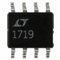
LT1719CS8 Linear Technology, LT1719CS8 Datasheet - Page 10

LT1719CS8
Manufacturer Part Number
LT1719CS8
Description
IC COMP R-R I/O SGL 3/5V 8-SOIC
Manufacturer
Linear Technology
Series
UltraFast™r
Type
General Purposer
Datasheet
1.LT1719CS8PBF.pdf
(22 pages)
Specifications of LT1719CS8
Number Of Elements
1
Output Type
CMOS, Rail-to-Rail, TTL
Voltage - Supply
2.7 V ~ 10.5 V
Mounting Type
Surface Mount
Package / Case
8-SOIC (0.154", 3.90mm Width)
Lead Free Status / RoHS Status
Contains lead / RoHS non-compliant
Other names
Q1357287
Available stocks
Company
Part Number
Manufacturer
Quantity
Price
Part Number:
LT1719CS8
Manufacturer:
LINEAR/凌特
Quantity:
20 000
Company:
Part Number:
LT1719CS8#PBF
Manufacturer:
LT
Quantity:
39
Part Number:
LT1719CS8#PBF
Manufacturer:
LINEAR/凌特
Quantity:
20 000
Company:
Part Number:
LT1719CS8#TRPBF
Manufacturer:
LT
Quantity:
9 200
Part Number:
LT1719CS8#TRPBF
Manufacturer:
LINEAR/凌特
Quantity:
20 000
APPLICATIONS INFORMATION
LT1719
The propagation delay does not increase signifi cantly when
driven with large differential voltages, but with low levels
of overdrive, an apparent increase may be seen with large
source resistances due to an RC delay caused by the 2pF
typical input capacitance.
Input Protection
The input stage is protected against damage from large
differential signals, up to and beyond a differential voltage
equal to the supply voltage, limited only by the absolute
maximum currents noted. External input protection cir-
cuitry is only needed if currents would otherwise exceed
these absolute maximums. The internal catch diodes can
conduct current up to these rated maximums without
latchup, even when the supply voltage is at the absolute
maximum rating.
The LT1719 input stage has general purpose internal ESD
protection for the human body model. For use as a line
receiver, additional external protection may be required.
As with most integrated circuits, the level of immunity to
ESD is much greater when residing on a printed circuit
board where the power supply decoupling capacitance will
limit the voltage rise caused by an ESD pulse.
Input Bias Current
Input bias current is measured with both inputs held at
1V. As with any PNP differential input stage, the LT1719
bias current fl ows out of the device. It will go to zero
on the higher of the two inputs and double on the lower
of the two inputs. With more than two diode drops of
differential input voltage, the LT1719’s input protection
circuitry activates, and current out of the lower input will
increase an additional 30% and there will be a small bias
current into the higher of the two input pins, of 4μA or
less. See the Typical Performance curve Input Current vs
Differential Input Voltage.
High Speed Design Considerations
Application of high speed comparators is often plagued by
oscillations. The LT1719 has 4mV of internal hysteresis,
which will prevent oscillations as long as parasitic output
10
to input feedback is kept below 4mV. However, with the
2V/ns slew rate of the LT1719 outputs, a 4mV step can
be created at a 100Ω input source with only 0.02pF of
output to input coupling. The LT1719’s pinout has been
arranged to minimize problems by placing the sensitive
inputs away from the outputs, shielded by the power rails.
The input and output traces of the circuit board should
also be separated, and the requisite level of isolation is
readily achieved if a topside ground plane runs between
the output and the inputs. For multilayer boards where the
ground plane is internal, a topside ground or supply trace
should be run between the inputs and the output.
Figure 2 shows a typical topside layout of the LT1719S8
on such a multilayer board. Shown is the topside metal
etch including traces, pin escape vias, and the land pads
for an SO-8 LT1719 and its adjacent X7R 10nF bypass
capacitors in the 1206 case. The same principles should
be used with the SOT 23-6.
The ground trace from Pin 5 runs under the device up
to the bypass capacitor, shielding the inputs from the
outputs. Note the use of a common via for the LT1719
and the bypass capacitors, which minimizes interference
from high frequency energy running around the ground
plane or power distribution traces.
The supply bypass should include an adjacent
10nF ceramic capacitor and a 2.2μF tantalum capacitor
no farther than 5cm away; use more capacitance on + V
if driving more than 4mA loads. To prevent oscillations,
it is helpful to balance the impedance at the inverting and
noninverting inputs; source impedances should be kept
low, preferably 1kΩ or less.
Figure 2. Typical Topside Metal for Multilayer PCB Layouts
1719 F02
1719fa
S


