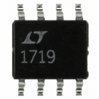
LT1719CS8 Linear Technology, LT1719CS8 Datasheet - Page 18

LT1719CS8
Manufacturer Part Number
LT1719CS8
Description
IC COMP R-R I/O SGL 3/5V 8-SOIC
Manufacturer
Linear Technology
Series
UltraFast™r
Type
General Purposer
Datasheet
1.LT1719CS8PBF.pdf
(22 pages)
Specifications of LT1719CS8
Number Of Elements
1
Output Type
CMOS, Rail-to-Rail, TTL
Voltage - Supply
2.7 V ~ 10.5 V
Mounting Type
Surface Mount
Package / Case
8-SOIC (0.154", 3.90mm Width)
Lead Free Status / RoHS Status
Contains lead / RoHS non-compliant
Other names
Q1357287
Available stocks
Company
Part Number
Manufacturer
Quantity
Price
Part Number:
LT1719CS8
Manufacturer:
LINEAR/凌特
Quantity:
20 000
Company:
Part Number:
LT1719CS8#PBF
Manufacturer:
LT
Quantity:
39
Part Number:
LT1719CS8#PBF
Manufacturer:
LINEAR/凌特
Quantity:
20 000
Company:
Part Number:
LT1719CS8#TRPBF
Manufacturer:
LT
Quantity:
9 200
Part Number:
LT1719CS8#TRPBF
Manufacturer:
LINEAR/凌特
Quantity:
20 000
LT1719
APPLICATIONS INFORMATION
±V
The input trip points test circuit uses a 1kHz triangle wave
to repeatedly trip the comparator being tested. The LT1719
output is used to trigger switched capacitor sampling of the
triangle wave, with a sampler for each direction. Because the
triangle wave is attenuated 1000:1 and fed to the LT1719’s
differential input, the sampled voltages are therefore 1000
times the input trip voltages. The hysteresis and offset are
computed from the trip points as shown.
Crystal Oscillator
A simple crystal oscillator using an LT1719 is shown on
the fi rst page of this data sheet. The 2k-620Ω resistor pair
set a bias point at the comparator’s noninverting input.
The 2k-1.8k-0.1μF path sets the inverting input node at
an appropriate DC average level based on the output.
The crystal’s path provides resonant positive feedback
and stable oscillation occurs. Although the LT1719 will
give the correct logic output when one input is outside
the common mode range, additional delays may occur
when it is so operated, opening the possibility of spurious
operating modes. Therefore, the DC bias voltages at the
inputs are set near the center of the LT1719’s common
18
TRIP
Test Circuit
2.7V TO 6V
V
Figure 8. Crystal Oscillator with a Forced 50% Duty Cycle
CC
620Ω
2k
220Ω
+
–
CRYSTAL (AT-CUT)
LT1719
1MHz TO 10MHz
C1
0.1μF
GROUND
CASE
1.8k
2k
1k
mode range and the 220Ω resistor attenuates the feedback
to the noninverting input. The circuit will operate with any
AT-cut crystal from 1MHz to 10MHz over a 2.7V to 6V sup-
ply range. As the power is applied, the circuit remains off
until the LT1719 bias circuits activate, at a typical V
2V to 2.2V (25°C), at which point the desired frequency
output is generated.
The output duty cycle of this circuit is roughly 50%, but
it is affected by resistor tolerances and to a lesser extent,
by comparator offsets and timings. If a 50% duty cycle is
required, the circuit of Figure 8 forces a 50% duty cycle.
Crystals are narrow-band elements, so the feedback to
the noninverting input is a fi ltered analog version of the
square wave output. Changing the noninverting reference
level can therefore vary the duty cycle. C1 operates as in
the previous example while A1 compares a band-limited
version of the output and biases C1’s negative input. C1’s
only degree of freedom to respond is variation of pulse
width; hence the output is forced to 50% duty cycle.
Again, the circuit operates from 2.7V to 6V. There is a
slight duty cycle dependence on comparator loading, so
minimal capacitive and resistive loading should be used
in critical applications.
0.1μF
LT1636
A1
+
–
200k
200k
100k
0.1μF
OUTPUT
V
CC
1720 F07
CC
1719fa
of


