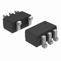
LMV331SQ3T2G ON Semiconductor, LMV331SQ3T2G Datasheet - Page 11

LMV331SQ3T2G
Manufacturer Part Number
LMV331SQ3T2G
Description
IC COMPARATOR GP LV SINGLE SC-70
Manufacturer
ON Semiconductor
Type
General Purposer
Datasheet
1.LMV331SQ3T2G.pdf
(21 pages)
Specifications of LMV331SQ3T2G
Number Of Elements
1
Output Type
Open Drain
Voltage - Supply
2.7 V ~ 5 V
Mounting Type
Surface Mount
Package / Case
6-TSSOP (5 lead), SC-88A, SOT-353
Product
Analog Comparators
Lead Free Status / RoHS Status
Lead free / RoHS Compliant
Available stocks
Company
Part Number
Manufacturer
Quantity
Price
Company:
Part Number:
LMV331SQ3T2G
Manufacturer:
ON
Quantity:
15 000
Company:
Part Number:
LMV331SQ3T2G
Manufacturer:
ON Semiconductor
Quantity:
1 950
Part Number:
LMV331SQ3T2G
Manufacturer:
ON/安森美
Quantity:
20 000
Basic Comparator Operation
input voltage signals, and produce a digital output signal by
determining which input signal is higher. If the voltage on
the non−inverting input is higher, then the internal output
transistor is off and the output will be high. If the voltage on
the inverting input is higher, then the output transistor will
be on and the output will be low. The LMV331/393/339 has
an open−drain output stage, so a pull−up resistor to a positive
supply voltage is required for the output to switch properly.
between 1 kW and 10 kW. This range of values will balance
two key factors; i.e., power dissipation and drive capability
for interface circuitry.
and assumes dual supplies. The comparator compares the
input voltage (V
reference voltage (V
than V
greater than V
Comparators and Stability
their high gain. The basic comparator configuration in
Figure 19 may oscillate if the differential voltage between
the input pins is close to the device’s offset voltage. This can
happen if the input signal is moving slowly through the
comparator’s switching threshold or if unused channels are
connected to the same potential for termination of unused
channels. One way to eliminate output oscillations or
‘chatter’ is to include external hysteresis in the circuit
design.
Inverting Configuration with Hysteresis
Figure 20.
V
The basic operation of a comparator is to compare two
The size of the pull−up resistor is recommended to be
Figure 19 illustrates the basic operation of a comparator
A common problem with comparators is oscillation due to
An inverting comparator with hysteresis is shown in
REF
0 V
V
+V
+
+V
REF
REF
IN
, the output voltage (V
REF
V
, then V
IN
+
−
IN
) on the non−inverting input to the
REF
V
OUT
Figure 19.
) on the inverting input. If V
O
will be high.
O
) will be low. If V
V
+
3.0 k
APPLICATION CIRCUITS
V
Time
O
IN
http://onsemi.com
is less
IN
is
11
node, V
greater than the voltage at V
The hysteresis band (Figure 21) created from the resistor
network is defined as:
where V
respectively.
comparator is pulled up to supply when high. The
resistances R
which is in series with R
comparator is at ground potential when low. The resistances
R
series with R
2
When V
V
V
and R
T1
T2
V
IN
is calculated by assuming that the output of the
is calculated by assuming that the output of the
R
V
R
+
T1
, the output voltage will be high. When V
+
3
1
2
IN
V
V
can be viewed as being in parallel which is in
and V
O
CC
1
1
is less than the voltage at the non−inverting
0
(Figure 23). Therefore V
and R
−
+
V
V
T2
V
DV
T2
T1
Figure 20. Inverting
T2
are the lower and upper trip points,
Figure 21.
3
Comparator with
+
+
+V
)
can be viewed as being in parallel
R3
2
Hysteresis
+ V
R
CC
R
(Figure 22). Therefore V
V
V
1
IN
CC
1
) R
+
V
ø R
T1
, then the output will be low.
CC
R
* V
3
2
2
R
ø R
) R
ø R
V
2
T2
T1
3
3
2
T2
R
PULL−UP
is:
V
R
O
LOAD
T1
IN
is:
is


