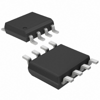
MAX9022ASA+ Maxim Integrated Products, MAX9022ASA+ Datasheet - Page 2

MAX9022ASA+
Manufacturer Part Number
MAX9022ASA+
Description
IC COMPARATOR DUAL 8-SOIC
Manufacturer
Maxim Integrated Products
Type
General Purposer
Datasheet
1.MAX9022AKAT.pdf
(8 pages)
Specifications of MAX9022ASA+
Number Of Elements
2
Output Type
CMOS, Rail-to-Rail, TTL
Voltage - Supply
2.5 V ~ 5.5 V, ±1.25 V ~ 2.75 V
Mounting Type
Surface Mount
Package / Case
8-SOIC (0.154", 3.90mm Width)
Number Of Channels
2 Channels
Product
Digital Comparators
Offset Voltage (max)
+/- 8 mV
Input Bias Current (max)
80 nA
Supply Voltage (max)
5.5 V
Supply Voltage (min)
2.5 V
Supply Current (max)
5 uA
Maximum Power Dissipation
471 mW
Maximum Operating Temperature
+ 125 C
Mounting Style
SMD/SMT
Minimum Operating Temperature
- 40 C
Lead Free Status / RoHS Status
Lead free / RoHS Compliant
ABSOLUTE MAXIMUM RATINGS
Supply Voltage (V
Voltage Inputs (IN+, IN- to V
Differential Input Voltage (IN+ to IN-)....................................6.6V
Current into Input Pins ......................................................±20mA
Output Short-Circuit Duration ..................2s to Either V
Current into Any Pin ............................................................20mA
Continuous Power Dissipation (T
ELECTRICAL CHARACTERISTICS
(V
Micropower, Ultra-Small, Single/Dual/Quad,
Single-Supply Comparators
Stresses beyond those listed under “Absolute Maximum Ratings” may cause permanent damage to the device. These are stress ratings only, and functional
operation of the device at these or any other conditions beyond those indicated in the operational sections of the specifications is not implied. Exposure to
absolute maximum rating conditions for extended periods may affect device reliability.
2
Note 1: All devices are production tested at 25°C. All temperature limits are guaranteed by design.
Note 2: Comparator Input Offset is defined as the center of the hysteresis zone.
Note 3: Hysteresis is defined as the difference of the trip points required to change comparator output states.
Note 4: V
Note 5: Rise and fall times are measured between 10% and 90% at OUT.
Operating Voltage Range
S up p l y C ur r ent P er C om p ar ator
Input Offset Voltage
Input Offset Voltage
Temperature Coefficient
Hysteresis
Input Bias Current
Input Offset Current
Common-Mode Voltage Range
C om m on- M od e Rej ecti on Rati o
Power-Supply Rejection Ratio
Output-Voltage Swing
Output Short-Circuit Current
Propagation Delay
Rise and Fall Time
Power-On Time
Maximum Capacitive Load
5-Pin SC70 (derate 3.1mW/°C above +70°C) ...............247mW
5-Pin SOT23 (derate 7.1mW/°C above +70°C).............571mW
8-Pin SOT23 (derate 9.1mW/°C above +70°C).............727mW
DD
_______________________________________________________________________________________
= 5V, V
OD
PARAMETER
SS
is the overdrive voltage beyond the offset and hysteresis-determined trip points.
= 0, V
DD
to V
CM
SS
= 0, T
) ....................................-0.3V to +6V
SS
). ................-0.3V to (V
A
A
= -40°C to +125°C, unless otherwise noted. Typical values are at T
= +70°C)
SYMBOL
V
t
pd+
TCV
CMRR
OL
PSRR
I
t
V
V
V
I
BIAS
R
I
I
C
DD
OS
SC
CM
, V
DD
OS
, t
, t
L
OS
pd
F
OH
-
Guaranteed by PSRR test
(Note 2)
(Note 3)
Guaranteed by CMRR test
V
V
V
(V
V
(V
R
C
R
R
No sustained oscillations
S S
DD
OH
OL
L
L
L
L
IN+
IN-
= 10kΩ,
= 10kΩ, C
= 10kΩ, C
= 15pF (Note 4)
DD
≤ V
= 2.5V to 5.5V
= V
DD
= V
- V
- V
C M
+ 0.3V)
OUT
IN+
or V
DD
IN-
≤ ( V
) ≥ 20mV
) ≥ 20mV
- V
SS
- V
L
L
D D
OUT,
= 15pF (Note 5)
= 15pF
CONDITIONS
SS,
- 1.1V ) , V
Operating Temperature Range
Junction Temperature ......................................................+150°C
Storage Temperature Range .............................-65°C to +150°C
Lead Temperature (soldering, 10s) .................................+300°C
8-Pin µMAX (derate 4.5mW/°C above +70°C) ..............362mW
8-Pin SO (derate 5.88mW/°C above +70°C).................471mW
14-Pin TSSOP (derate 9.1mW/°C above +70°C) ..........727mW
14-Pin SO (derate 8.3mW/°C above +70.......................667mW
Automotive Application...................................-40°C to +125°C
V
V
I
I
I
I
SOURCE
SOURCE
SINK
SINK
OD
OD
D D
= 5.5V
= 10mV
= 100mV
= 10µA
= 4mA
= 10µA
= 4mA
MIN
V
2.5
60
70
SS
A
= +25°C.) (Note 1)
TYP
160
180
150
150
100
2.8
±1
±1
±2
80
50
20
4
3
2
2
8
3
V
DD
MAX
±60
400
400
5.5
±8
80
5
- 1.1
UNITS
µV/°C
mV
mV
mV
m A
dB
µA
nA
nA
d B
pF
µs
ns
ns
V
V


