MAX3815CCM+TD Maxim Integrated Products, MAX3815CCM+TD Datasheet - Page 6
MAX3815CCM+TD
Manufacturer Part Number
MAX3815CCM+TD
Description
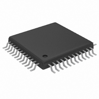
IC EQUALIZER VIDEO 48-TQFP
Manufacturer
Maxim Integrated Products
Type
Video Equalizerr
Datasheet
1.MAX3815CCMTD.pdf
(11 pages)
Specifications of MAX3815CCM+TD
Applications
HDMI, DVI, Receivers
Mounting Type
Surface Mount
Package / Case
48-TQFP Exposed Pad, 48-eTQFP, 48-HTQFP, 48-VQFP
Lead Free Status / RoHS Status
Lead free / RoHS Compliant


The MAX3815 TMDS equalizer accepts differential CML
input data at rates of 250Mbps up to 1.65Gbps (individ-
ual channel data rate). It automatically adjusts to atten-
uation levels of up to 40dB at 825MHz due to
skin-effect losses in copper cable. It consists of four
CML input buffers, a loss-of-clock signal detector, three
independent adaptive equalizers, four limiting ampli-
fiers, and four output buffers (Figure 1).
The input buffers and the output drivers are implement-
ed using current-mode logic (CML) (see Figures 3 and
4). The output drivers are open-collector and can be
turned off with the OUTON pin, or can be set to output
a one-half amplitude signal (500mV
using the OUTLEVEL pin. For details on interfacing with
CML, refer to Maxim Application Note HFAN-01.0:
Introduction to LVDS, PECL, and CML .
The loss-of-clock signal detector indicates a loss-of-
clock signal at the CLKLOS pin.
TMDS Digital Video Equalizer for DVI/HDMI
Cables
6
20, 23, 24,
25, 28, 29,
32, 33, 36,
_______________________________________________________________________________________
37, 42
45–48
PIN
EP
21
22
26
27
30
31
34
35
39
40
CML Input Buffers and Output Drivers
Exposed Pad
RXC_OUT+
RX2_OUT+
RX1_OUT+
RX0_OUT+
OUTLEVEL
RXC_OUT-
RX2_OUT-
RX1_OUT-
RX0_OUT-
OUTON
Loss-of-Clock Signal Detector
NAME
GND
N.C.
Detailed Description
Ground
Negative Clock Output, CML
Positive Clock Output, CML
Positive Data Output, CML
Negative Data Output, CML
Positive Data Output, CML
Negative Data Output, CML
Positive Data Output, CML
Negative Data Output, CML
Output-Level Control Input, LVTTL. This input sets the output amplitude to the standard DVI level
(1000mV
Output-Enable Control Input, LVTTL. This input enables the CML outputs when forced low and sets a
differential logic zero when forced high.
No Connection
Ground. The exposed pad must be soldered to the circuit-board ground for proper
thermal and electrical operation.
P-P
) when high, and sets the output amplitude to 1/2 the DVI level (500mV
P-P
differential)
The three data channels each contain an independent
adaptive equalizer. Each channel analyzes the incom-
ing signal and determines the amount of equalization to
apply.
The limiting amplifier amplifies the signal from the
adaptive equalizer and truncates the top and bottom of
the waveform to provide a clean high- and low-level
signal to the output drivers.
Typical shielded twisted pair (STP) and unshielded
twisted pair (UTP) cables exhibit skin-effect losses,
which attenuate the high-frequency spectrum of a
TMDS signal, eventually causing data errors or even
closing the signal eye altogether given a long enough
cable. The MAX3815 recovers the data and opens the
signal eye through compensating equalization.
The basic TMDS interface is composed of four differen-
tial serial links: three links carry serial data up to
1.65Gbps each, and the fourth is a one-tenth-rate
(0.1x) clock that operates up to 165MHz. TMDS, as with
FUNCTION
Pin Description (continued)
Applications Information
Adaptive Equalizer
Limiting Amplifier
P-P
) when low.
Related parts for MAX3815CCM+TD
Image
Part Number
Description
Manufacturer
Datasheet
Request
R

Part Number:
Description:
MAX7528KCWPMaxim Integrated Products [CMOS Dual 8-Bit Buffered Multiplying DACs]
Manufacturer:
Maxim Integrated Products
Datasheet:
Part Number:
Description:
Single +5V, fully integrated, 1.25Gbps laser diode driver.
Manufacturer:
Maxim Integrated Products
Datasheet:
Part Number:
Description:
Single +5V, fully integrated, 155Mbps laser diode driver.
Manufacturer:
Maxim Integrated Products
Datasheet:
Part Number:
Description:
VRD11/VRD10, K8 Rev F 2/3/4-Phase PWM Controllers with Integrated Dual MOSFET Drivers
Manufacturer:
Maxim Integrated Products
Datasheet:
Part Number:
Description:
Highly Integrated Level 2 SMBus Battery Chargers
Manufacturer:
Maxim Integrated Products
Datasheet:
Part Number:
Description:
Current Monitor and Accumulator with Integrated Sense Resistor; ; Temperature Range: -40°C to +85°C
Manufacturer:
Maxim Integrated Products
Part Number:
Description:
TSSOP 14/A�/RS-485 Transceivers with Integrated 100O/120O Termination Resis
Manufacturer:
Maxim Integrated Products
Part Number:
Description:
TSSOP 14/A�/RS-485 Transceivers with Integrated 100O/120O Termination Resis
Manufacturer:
Maxim Integrated Products
Part Number:
Description:
QFN 16/A�/AC-DC and DC-DC Peak-Current-Mode Converters with Integrated Step
Manufacturer:
Maxim Integrated Products
Part Number:
Description:
TDFN/A/65V, 1A, 600KHZ, SYNCHRONOUS STEP-DOWN REGULATOR WITH INTEGRATED SWI
Manufacturer:
Maxim Integrated Products
Part Number:
Description:
Integrated Temperature Controller f
Manufacturer:
Maxim Integrated Products
Part Number:
Description:
SOT23-6/I�/45MHz to 650MHz, Integrated IF VCOs with Differential Output
Manufacturer:
Maxim Integrated Products
Part Number:
Description:
SOT23-6/I�/45MHz to 650MHz, Integrated IF VCOs with Differential Output
Manufacturer:
Maxim Integrated Products
Part Number:
Description:
EVALUATION KIT/2.4GHZ TO 2.5GHZ 802.11G/B RF TRANSCEIVER WITH INTEGRATED PA
Manufacturer:
Maxim Integrated Products
Part Number:
Description:
QFN/E/DUAL PCIE/SATA HIGH SPEED SWITCH WITH INTEGRATED BIAS RESISTOR
Manufacturer:
Maxim Integrated Products
Datasheet: