NLU1GT50MUTCG ON Semiconductor, NLU1GT50MUTCG Datasheet - Page 2
NLU1GT50MUTCG
Manufacturer Part Number
NLU1GT50MUTCG
Description
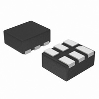
IC BUFFER TTL NON-INVERT 6UDFN
Manufacturer
ON Semiconductor
Datasheet
1.NLU1GT50MUTCG.pdf
(8 pages)
Specifications of NLU1GT50MUTCG
Logic Type
Buffer/Line Driver, Non-Inverting
Number Of Elements
1
Number Of Bits Per Element
1
Current - Output High, Low
8mA, 8mA
Voltage - Supply
1.65 V ~ 3.6 V
Operating Temperature
-55°C ~ 125°C
Mounting Type
Surface Mount
Package / Case
6-UFDFN
Number Of Channels Per Chip
1
Polarity
Non-Inverting
Supply Voltage (max)
5.5 V
Supply Voltage (min)
1.65 V
Maximum Operating Temperature
+ 125 C
Mounting Style
SMD/SMT
High Level Output Current
- 8 mA
Low Level Output Current
8 mA
Minimum Operating Temperature
- 55 C
Number Of Lines (input / Output)
1 / 1
Propagation Delay Time
19.5 ns at 2.3 V to 2.7 V, 13.5 ns at 3 V to 3.6 V, 7.7 ns at 4.5 V to 5.5 V
Lead Free Status / RoHS Status
Lead free / RoHS Compliant
Other names
NLU1GT50MUTCGOSTR
Available stocks
Company
Part Number
Manufacturer
Quantity
Price
Company:

Part Number:
NLU1GT50MUTCG
Manufacturer:
ON Semiconductor
Quantity:
2 200


Stresses exceeding Maximum Ratings may damage the device. Maximum Ratings are stress ratings only. Functional operation above the
Recommended Operating Conditions is not implied. Extended exposure to stresses above the Recommended Operating Conditions may affect
device reliability.
1. Measured with minimum pad spacing on an FR4 board, using 10 mm-by-1 inch, 2 ounce copper trace no air flow.
2. Tested to EIA / JESD22-A114-A.
3. Tested to EIA / JESD22-A115-A.
4. Tested to JESD22-C101-A.
5. Tested to EIA / JESD78.
RECOMMENDED OPERATING CONDITIONS
MAXIMUM RATINGS
I
LATCHUP1
Symbol
Symbol
Dt/DV
V
T
V
V
I
MSL
V
V
GND
V
I
I
V
STG
T
F
T
OUT
I
T
ESD
OUT
OK
I
CC
CC
IK
CC
O
IN
IN
R
A
L
J
Positive DC Supply Voltage
Digital Input Voltage
Output Voltage
Operating Free-Air Temperature
Input Transition Rise or Fall Rate
DC Supply Voltage
DC Input Voltage
DC Output Voltage
DC Input Diode Current
DC Output Diode Current
DC Output Source/Sink Current
DC Supply Current Per Supply Pin
DC Ground Current per Ground Pin
Storage Temperature Range
Lead Temperature, 1 mm from Case for 10 Seconds
Junction Temperature Under Bias
Moisture Sensitivity
Flammability Rating Oxygen
ESD Withstand Voltage
Latchup Performance Above V
CC
and Below GND at 125 °C (Note 5)
Parameter
Parameter
Charged Device Model (Note 4)
Human Body Model (Note 2)
http://onsemi.com
NLU1GT50
Machine Model (Note 3)
V
V
CC
CC
2
= 3.3 V ± 0.3 V
= 5.0 V ± 0.5 V
Index: 28 to 34
V
OUT
V
IN
< GND
< GND
UL 94 V-0 @ 0.125 in
1.65
Min
-55
0
0
0
0
-0.5 to +7.0
-0.5 to +7.0
-0.5 to +7.0
-65 to +150
Level 1
> 2000
Value
±12.5
> 200
±500
-20
±20
±25
±25
260
150
N/A
+125
Max
100
5.5
5.5
5.5
20
ns/V
Unit
Unit
mA
mA
mA
mA
mA
mA
°C
°C
°C
°C
V
V
V
V
V
V
V
Related parts for NLU1GT50MUTCG
Image
Part Number
Description
Manufacturer
Datasheet
Request
R

Part Number:
Description:
Non-inverting Buffer With Ttl-compatible Inputs
Manufacturer:
ON Semiconductor
Datasheet:
Part Number:
Description:
ON Semiconductor [VOLTAGE REGULATOR]
Manufacturer:
ON Semiconductor
Datasheet:
Part Number:
Description:
357-036-542-201 CARDEDGE 36POS DL .156 BLK LOPRO
Manufacturer:
ON Semiconductor
Datasheet:
Part Number:
Description:
357-036-542-201 CARDEDGE 36POS DL .156 BLK LOPRO
Manufacturer:
ON Semiconductor
Datasheet:
Part Number:
Description:
357-036-542-201 CARDEDGE 36POS DL .156 BLK LOPRO
Manufacturer:
ON Semiconductor
Datasheet:
Part Number:
Description:
357-036-542-201 CARDEDGE 36POS DL .156 BLK LOPRO
Manufacturer:
ON Semiconductor
Datasheet:
Part Number:
Description:
357-036-542-201 CARDEDGE 36POS DL .156 BLK LOPRO
Manufacturer:
ON Semiconductor
Datasheet:
Part Number:
Description:
357-036-542-201 CARDEDGE 36POS DL .156 BLK LOPRO
Manufacturer:
ON Semiconductor
Datasheet:
Part Number:
Description:
357-036-542-201 CARDEDGE 36POS DL .156 BLK LOPRO
Manufacturer:
ON Semiconductor
Datasheet:
Part Number:
Description:
357-036-542-201 CARDEDGE 36POS DL .156 BLK LOPRO
Manufacturer:
ON Semiconductor
Datasheet:
Part Number:
Description:
357-036-542-201 CARDEDGE 36POS DL .156 BLK LOPRO
Manufacturer:
ON Semiconductor
Datasheet:
Part Number:
Description:
357-036-542-201 CARDEDGE 36POS DL .156 BLK LOPRO
Manufacturer:
ON Semiconductor
Datasheet:
Part Number:
Description:
Manufacturer:
ON Semiconductor
Datasheet:
Part Number:
Description:
Manufacturer:
ON Semiconductor
Datasheet: