NLU1GT50MUTCG ON Semiconductor, NLU1GT50MUTCG Datasheet - Page 4
NLU1GT50MUTCG
Manufacturer Part Number
NLU1GT50MUTCG
Description
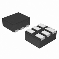
IC BUFFER TTL NON-INVERT 6UDFN
Manufacturer
ON Semiconductor
Datasheet
1.NLU1GT50MUTCG.pdf
(8 pages)
Specifications of NLU1GT50MUTCG
Logic Type
Buffer/Line Driver, Non-Inverting
Number Of Elements
1
Number Of Bits Per Element
1
Current - Output High, Low
8mA, 8mA
Voltage - Supply
1.65 V ~ 3.6 V
Operating Temperature
-55°C ~ 125°C
Mounting Type
Surface Mount
Package / Case
6-UFDFN
Number Of Channels Per Chip
1
Polarity
Non-Inverting
Supply Voltage (max)
5.5 V
Supply Voltage (min)
1.65 V
Maximum Operating Temperature
+ 125 C
Mounting Style
SMD/SMT
High Level Output Current
- 8 mA
Low Level Output Current
8 mA
Minimum Operating Temperature
- 55 C
Number Of Lines (input / Output)
1 / 1
Propagation Delay Time
19.5 ns at 2.3 V to 2.7 V, 13.5 ns at 3 V to 3.6 V, 7.7 ns at 4.5 V to 5.5 V
Lead Free Status / RoHS Status
Lead free / RoHS Compliant
Other names
NLU1GT50MUTCGOSTR
Available stocks
Company
Part Number
Manufacturer
Quantity
Price
Company:

Part Number:
NLU1GT50MUTCG
Manufacturer:
ON Semiconductor
Quantity:
2 200


6. C
†For information on tape and reel specifications, including part orientation and tape sizes, please refer to our Tape and Reel Packaging
ORDERING INFORMATION
NLU1GT50MUTCG
NLU1GT50AMX1TCG
NLU1GT50BMX1TCG
NLU1GT50CMX1TCG
Specifications Brochure, BRD8011/D.
AC ELECTRICAL CHARACTERISTICS
Symbol
t
load. Average operating current can be obtained by the equation I
dynamic power consumption: P
t
C
PLH
C
PHL
PD
PD
IN
,
is defined as the value of the internal equivalent capacitance which is calculated from the dynamic operating current consumption without
Propagation Delay,
Input A to Output Y
Input Capacitance
Power Dissipation
Capacitance (Note 6)
Device
Parameter
D
= C
PD
1.65 to 1.95
• V
2.3 to 2.7
3.0 to 3.6
4.5 to 5.5
V
CC
A
Y
CC
5.0
(Input t
(V)
2
*Includes all probe and jig capacitance
Figure 3. Switching Waveforms
50%
• f
in
r
ULLGA6, 1.45 x 1.0, 0.5P
ULLGA6, 1.0 x 1.0, 0.35P
+ I
ULLGA6, 1.2 x 1.0, 0.4P
DEVICE
UNDER
= t
Figure 4. Test Circuit
TEST
CC
C
C
C
C
C
C
C
http://onsemi.com
Condition
f
= 3.0 n)
L
L
L
L
L
L
L
• V
Test
= 15 pF
= 15 pF
= 50 pF
= 15 pF
= 50 pF
= 15 pF
= 50 pF
NLU1GT50
(Pb-Free)
(Pb-Free)
(Pb-Free)
(Pb-Free)
Package
CC
UDFN6
50% V
t
PLH
.
4
CC(OPR)
OUTPUT
CC
Min
TEST POINT
= C
T
A
PD
= 25 5C
Typ
4.5
6.3
3.5
4.3
t
12
PHL
5
C
• V
L
*
CC
V
GND
V
V
CC
OH
OL
Max
16.6
13.3
19.5
10.0
13.5
• f
6.7
7.7
10
in
+ I
CC
Min
T
. C
A
= +855C
PD
is used to determine the no-load
Max
18.0
14.5
22.0
11.0
15.0
3000 / Tape & Reel
3000 / Tape & Reel
3000 / Tape & Reel
3000 / Tape & Reel
7.5
8.5
10
Shipping
Min
T
to +1255C
A
= -555C
†
Max
22.0
17.5
25.5
13.0
17.5
10.0
8.5
9.5
Unit
pF
pF
ns
Related parts for NLU1GT50MUTCG
Image
Part Number
Description
Manufacturer
Datasheet
Request
R

Part Number:
Description:
Non-inverting Buffer With Ttl-compatible Inputs
Manufacturer:
ON Semiconductor
Datasheet:
Part Number:
Description:
ON Semiconductor [VOLTAGE REGULATOR]
Manufacturer:
ON Semiconductor
Datasheet:
Part Number:
Description:
357-036-542-201 CARDEDGE 36POS DL .156 BLK LOPRO
Manufacturer:
ON Semiconductor
Datasheet:
Part Number:
Description:
357-036-542-201 CARDEDGE 36POS DL .156 BLK LOPRO
Manufacturer:
ON Semiconductor
Datasheet:
Part Number:
Description:
357-036-542-201 CARDEDGE 36POS DL .156 BLK LOPRO
Manufacturer:
ON Semiconductor
Datasheet:
Part Number:
Description:
357-036-542-201 CARDEDGE 36POS DL .156 BLK LOPRO
Manufacturer:
ON Semiconductor
Datasheet:
Part Number:
Description:
357-036-542-201 CARDEDGE 36POS DL .156 BLK LOPRO
Manufacturer:
ON Semiconductor
Datasheet:
Part Number:
Description:
357-036-542-201 CARDEDGE 36POS DL .156 BLK LOPRO
Manufacturer:
ON Semiconductor
Datasheet:
Part Number:
Description:
357-036-542-201 CARDEDGE 36POS DL .156 BLK LOPRO
Manufacturer:
ON Semiconductor
Datasheet:
Part Number:
Description:
357-036-542-201 CARDEDGE 36POS DL .156 BLK LOPRO
Manufacturer:
ON Semiconductor
Datasheet:
Part Number:
Description:
357-036-542-201 CARDEDGE 36POS DL .156 BLK LOPRO
Manufacturer:
ON Semiconductor
Datasheet:
Part Number:
Description:
357-036-542-201 CARDEDGE 36POS DL .156 BLK LOPRO
Manufacturer:
ON Semiconductor
Datasheet:
Part Number:
Description:
Manufacturer:
ON Semiconductor
Datasheet:
Part Number:
Description:
Manufacturer:
ON Semiconductor
Datasheet: