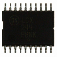
MC74LCX244DTG ON Semiconductor, MC74LCX244DTG Datasheet - Page 4

MC74LCX244DTG
Manufacturer Part Number
MC74LCX244DTG
Description
IC BUFF/DVR TRI-ST DUAL 20TSSOP
Manufacturer
ON Semiconductor
Series
74LCXr
Datasheet
1.MC74LCX244DTR2G.pdf
(10 pages)
Specifications of MC74LCX244DTG
Logic Type
Buffer/Line Driver, Non-Inverting
Number Of Elements
2
Number Of Bits Per Element
4
Current - Output High, Low
24mA, 24mA
Voltage - Supply
2 V ~ 3.6 V
Operating Temperature
-40°C ~ 85°C
Mounting Type
Surface Mount
Package / Case
20-TSSOP
Logic Family
74LCX
Number Of Channels Per Chip
Octal
Polarity
Non-Inverting
Supply Voltage (max)
3.6 V
Supply Voltage (min)
2 V
Maximum Operating Temperature
+ 85 C
Mounting Style
SMD/SMT
High Level Output Current
- 24 mA
Input Bias Current (max)
10 uA
Low Level Output Current
24 mA
Maximum Power Dissipation
200 mW
Minimum Operating Temperature
- 40 C
Number Of Lines (input / Output)
3
Output Type
3-State
Propagation Delay Time
7.5 ns @ 2.7 V or 6.5 ns @ 3 V to 3.6 V
Logic Device Type
Buffer, Non Inverting
Supply Voltage Range
2V To 3.6V
Logic Case Style
TSSOP
No. Of Pins
20
Operating Temperature Range
-40°C To +85°C
Filter Terminals
SMD
Rohs Compliant
Yes
Family Type
LCX
Logical Function
Buffer/Line Driver
Number Of Elements
2
Number Of Channels
8
Number Of Inputs
8
Number Of Outputs
8
Operating Supply Voltage (typ)
2.5/3.3V
Package Type
TSSOP
Operating Supply Voltage (max)
3.6V
Operating Supply Voltage (min)
2V
Quiescent Current
10uA
Technology
CMOS
Pin Count
20
Mounting
Surface Mount
Operating Temp Range
-55C to 125C
Operating Temperature Classification
Military
Lead Free Status / RoHS Status
Lead free / RoHS Compliant
Other names
MC74LCX244DTG
MC74LCX244DTGOS
MC74LCX244DTGOS
Available stocks
Company
Part Number
Manufacturer
Quantity
Price
Company:
Part Number:
MC74LCX244DTG
Manufacturer:
ON
Quantity:
375
2. These values of V
3. Skew is defined as the absolute value of the difference between the actual propagation delay for any two separate outputs of the same device.
DC ELECTRICAL CHARACTERISTICS
AC CHARACTERISTICS (t
t
t
t
t
t
t
t
t
Symbol
Symbol
V
V
V
V
I
I
I
I
DI
PLH
PHL
PZH
PZL
PHZ
PLZ
OSHL
OSLH
I
OZ
OFF
CC
IH
IL
OH
OL
The specification applies to any outputs switching in the same direction, either HIGH−to−LOW (t
guaranteed by design.
CC
Propagation Delay
Input to Output
Output Enable Time to
High and Low Level
Output Disable Time From
High and Low Level
Output−to−Output Skew
(Note 3)
HIGH Level Input Voltage (Note 2)
LOW Level Input Voltage (Note 2)
HIGH Level Output Voltage
LOW Level Output Voltage
Input Leakage Current
3−State Output Current
Power−Off Leakage Current
Quiescent Supply Current
Increase in I
I
Parameter
are used to test DC electrical characteristics only.
CC
per Input
Characteristic
R
= t
F
= 2.5 ns; R
Waveform
1
2
2
L
= 500 W)
http://onsemi.com
V
CC
2.3 ≤ V
Min
1.5
1.5
1.5
1.5
1.5
1.5
2.3 V ≤ V
2.3 ≤ V
2.3 ≤ V
2.3 ≤ V
= 3.0 V to 3.6 V
C
2.3 V ≤ V
2.3 V ≤ V
L
V
= 50 pF
4
V
V
V
CC
V
V
V
V
CC
CC
CC
CC
V
CC
CC
CC
CC
CC
CC
CC
CC
2.3 V ≤ V
2.7 V ≤ V
2.3 V ≤ V
2.7 V ≤ V
≤ 3.6 V; 3.6 ≤ V
CC
= 0 V; V
= 2.7 V; I
= 3.0 V; I
= 3.0 V; I
= 2.3 V; I
= 3.0 V; I
= 3.0 V; I
≤ 3.6 V; V
CC
CC
= 2.7 V; I
≤ 3.6 V; 0 V ≤ V
≤ 3.6 V; V
Max
V
= 2.3 V; I
6.5
6.5
8.0
8.0
7.0
7.0
1.0
1.0
I
≤ 3.6 V; 0 V ≤ V
Condition
= V
≤ 3.6 V; I
≤ 3.6 V; I
IH
I
CC
CC
CC
CC
or V
OH
OH
OH
OH
OL
OL
or V
OL
T
IH
OL
I
A
≤ 2.7 V
≤ 3.6 V
≤ 2.7 V
≤ 3.6 V
= GND or V
= −12 mA
= −18 mA
= −24 mA
= 12 mA
= 16 mA
= 24 mA
= −8 mA
O
= V
OL
OL
= 8 mA
= −55°C to +125°C
Min
1.5
1.5
1.5
1.5
1.5
1.5
I
IL
= 5.5 V
V
or V
C
= 100 mA
= 100 mA
CC
O
CC
L
Limits
I
≤ 5.5 V;
= 50 pF
O
≤ 5.5 V
− 0.6 V
= 2.7 V
≤ 5.5 V
OSHL
CC
Max
7.5
7.5
9.0
9.0
8.0
8.0
) or LOW−to−HIGH (t
V
T
CC
A
Min
1.7
2.0
1.8
2.2
2.4
2.2
= −55°C to +125°C
V
− 0.2
Min
1.5
1.5
1.5
1.5
1.5
1.5
CC
C
L
= 2.5 V +0.2
= 30 pF
Max
0.55
OSLH
±10
500
Max
0.7
0.8
0.2
0.6
0.4
0.4
±5
±5
10
10
7.8
7.8
8.4
8.4
10
10
); parameter
Unit
Unit
mA
mA
mA
mA
mA
ns
ns
ns
ns
V
V
V
V


