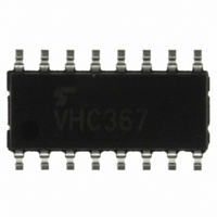
TC74VHC367FN(ELF,M) Toshiba, TC74VHC367FN(ELF,M) Datasheet

TC74VHC367FN(ELF,M)
Specifications of TC74VHC367FN(ELF,M)
Related parts for TC74VHC367FN(ELF,M)
TC74VHC367FN(ELF,M) Summary of contents
Page 1
... TOSHIBA CMOS Digital Integrated Circuit Silicon Monolithic TC74VHC367F,TC74VHC367FN,TC74VHC367FT,TC74VHC367FK TC74VHC368F,TC74VHC368FN,TC74VHC368FT,TC74VHC368FK Hex Bus Buffer TC74VHC367F/FN/FT Non-Inverted, 3-State TC74VHC368F/FN/FT Inverted, 3-State The TC74VHC367 and 368 are advanced high speed CMOS HEX BUS BUFFERs fabricated with silicon gate C technology. They achieve the high speed operation similar to equivalent Bipolar Schottky TTL while maintaining the CMOS low power dissipation ...
Page 2
Pin Assignment TC74VHC367 GND 8 (top view) IEC Logic Symbol TC74VHC367 ( (2) 1A (4) 2A (6) 3A (10) 4A (15) G ...
Page 3
Absolute Maximum Ratings (Note) Characteristics Supply voltage range DC input voltage DC output voltage Input diode current Output diode current DC output current DC V /ground current CC Power dissipation Storage temperature Note: Exceeding any of the absolute maximum ratings, ...
Page 4
Electrical Characteristics DC Characteristics Characteristics Symbol High-level input V IH voltage Low-level input V IL voltage High-level output V OH voltage Low-level output V OL voltage 3-state output I OZ off-state current Input leakage I IN current Quiescent supply I ...
Page 5
AC Characteristics (input Characteristics Symbol Propagation delay t pLH time t pHL (TC74VHC367) Propagation delay t pLH time t pHL (TC74VHC368) t pZL 3-state output enable R time t pZH t pLZ 3-state output disable R time t ...
Page 6
Input Equivalent Circuit INPUT TC74VHC367,368F/FN/FT/FK 6 2006-12-25 ...
Page 7
Package Dimensions Weight: 0.18 g (typ.) TC74VHC367,368F/FN/FT/FK 7 2006-12-25 ...
Page 8
Package Dimensions Weight: 0.18 g (typ.) TC74VHC367,368F/FN/FT/FK 8 2006-12-25 ...
Page 9
Package Dimensions (Note) Note: This package is not available in Japan. Weight: 0.13 g (typ.) TC74VHC367,368F/FN/FT/FK 9 2006-12-25 ...
Page 10
Package Dimensions Weight: 0.06 g (typ.) TC74VHC367,368F/FN/FT/FK 10 2006-12-25 ...
Page 11
Package Dimensions Weight: 0.02 g (typ.) TC74VHC367,368F/FN/FT/FK 11 2006-12-25 ...
Page 12
... The information contained herein is presented only as a guide for the applications of our products. No responsibility is assumed by TOSHIBA for any infringements of patents or other rights of the third parties which may result from its use. No license is granted by implication or otherwise under any patents or other rights of TOSHIBA or the third parties. • ...


