NL17SZ17DFT2G ON Semiconductor, NL17SZ17DFT2G Datasheet
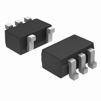
IC BUFF SCHMT TRG N-INV SOT353

NL17SZ17DFT2G

Manufacturer Part Number
NL17SZ17DFT2G
Description
IC BUFF SCHMT TRG N-INV SOT353
Manufacturer
ON Semiconductor
Series
17SZr
Datasheet

Specifications of NL17SZ17DFT2G

Logic Type
Schmitt Trigger - Buffer, Driver
Number Of Elements
1
Number Of Bits Per Element
1
Current - Output High, Low
32mA, 32mA
Voltage - Supply
1.65 V ~ 5.5 V
Operating Temperature
-40°C ~ 85°C
Mounting Type
Surface Mount
Package / Case
SC-70-5, SC-88A, SOT-323-5, SOT-353, 5-TSSOP
Logic Family
NL17SZ
Number Of Channels Per Chip
Single
Polarity
Non-Inverting
Supply Voltage (max)
5.5 V
Supply Voltage (min)
1.65 V
Maximum Operating Temperature
85 C
Mounting Style
SMD/SMT
High Level Output Current
- 32 mA
Input Bias Current (max)
1 uA
Low Level Output Current
32 mA
Maximum Power Dissipation
186 mW
Minimum Operating Temperature
- 40 C
Propagation Delay Time
7.2 ns @ 3.3 V or 5.9 ns @ 5 V
Number Of Lines (input / Output)
1 / 1
Logic Device Type
Buffer, Schmitt Trigger
Supply Voltage Range
1.65V To 5.5V
Logic Case Style
SOT-353
No. Of Pins
5
Operating Temperature Range
-40°C To +85°C
Filter Terminals
SMD
Rohs Compliant
Yes
Family Type
17SZ
Lead Free Status / RoHS Status
Lead free / RoHS Compliant
Other names
NL17SZ17DFT2GOS
NL17SZ17DFT2GOS
NL17SZ17DFT2GOSTR

Available stocks

Company
Part Number
Manufacturer
Quantity
Price
Part Number:
NL17SZ17DFT2G
Manufacturer:
ON
Quantity:
25 145
Part Number:
NL17SZ17DFT2G
Manufacturer:
ON/安森美
Quantity:
20 000
Part Number:
NL17SZ17DFT2G
0
Company:
Part Number:
NL17SZ17DFT2G
Quantity:
60 000
NL17SZ17
Single Non-Inverting Buffer
with Schmitt Trigger
two tiny footprint packages. The device performs much as LCX
multi−gate products in speed and drive.
Features
© Semiconductor Components Industries, LLC, 2010
August, 2010 − Rev. 8
The NL17SZ17 is a single Non−inverting Schmitt Trigger Buffer in
Tiny SOT−353 and SOT−553 Packages
Source/Sink 24 mA at 3.0 Volts
Overvoltage Tolerant Inputs and Outputs
Chip Complexity: FETs = 20
Designed for 1.65 V to 5.5 V V
Pb−Free Packages are Available
GND
NC
A
A
Figure 1. Pinout (Top View)
1
2
3
Figure 2. Logic Symbol
CC
Operation
5
4
Y
V
Y
CC
1
See detailed ordering and shipping information in the package
dimensions section on page 4 of this data sheet.
5
5
*Date Code orientation and/or position may
vary depending upon manufacturing location.
(Note: Microdot may be in either location)
1
A Input
1
ORDERING INFORMATION
Pin
1
2
3
4
5
H
L
LX = Specific Device Code
M = Date Code*
G = Pb−Free Package
(SC70−5/SC−88A)
http://onsemi.com
PIN ASSIGNMENT
FUNCTION TABLE
CASE 419A
DF SUFFIX
XV5 SUFFIX
SOT−353
CASE 463B
SOT−553
Publication Order Number:
Function
Y Output
DIAGRAMS
GND
5
1
V
MARKING
NC
A
Y
CC
1
5
NL17SZ17/D
H
L
LX MG
LX MG
G
G

Related parts for NL17SZ17DFT2G

NL17SZ17DFT2G Summary of contents

Page 1

NL17SZ17 Single Non-Inverting Buffer with Schmitt Trigger The NL17SZ17 is a single Non−inverting Schmitt Trigger Buffer in two tiny footprint packages. The device performs much as LCX multi−gate products in speed and drive. Features • Tiny SOT−353 and SOT−553 Packages ...

Page 2

MAXIMUM RATINGS Symbol V DC Supply Voltage Input Voltage Output Voltage Input Diode Current Output Diode Current Output Sink Current Supply Current ...

Page 3

DC ELECTRICAL CHARACTERISTICS Symbol Parameter V Positive Input ) T Threshold Voltage V Negative Input * T Threshold Voltage V Input Hysteresis Voltage H V High−Level Output Voltage ...

Page 4

... A Schmitt−Trigger Squares Up Inputs With Slow Rise and Fall Times DEVICE ORDERING INFORMATION Device Order Number NL17SZ17DFT2 NL17SZ17DFT2G NL17SZ17XV5T2 NL17SZ17XV5T2G †For information on tape and reel specifications, including part orientation and tape sizes, please refer to our Tape and Reel Packaging Specifications Brochure, BRD8011/D. *This package is inherently Pb−Free. ...

Page 5

... C H SOLDERING FOOTPRINT* 0.50 0.0197 0.40 0.0157 *For additional information on our Pb−Free strategy and soldering details, please download the ON Semiconductor Soldering and Mounting Techniques Reference Manual, SOLDERRM/D. DF SUFFIX CASE 419A−02 ISSUE J NOTES: 1. DIMENSIONING AND TOLERANCING PER ANSI Y14.5M, 1982. 2. CONTROLLING DIMENSION: INCH. ...

Page 6

... M *For additional information on our Pb−Free strategy and soldering details, please download the ON Semiconductor Soldering and Mounting Techniques Reference Manual, SOLDERRM/D. ON Semiconductor and are registered trademarks of Semiconductor Components Industries, LLC (SCILLC). SCILLC reserves the right to make changes without further notice to any products herein ...

Related keywords