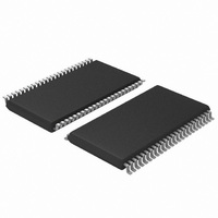
M74LCX16244DTR2G ON Semiconductor, M74LCX16244DTR2G Datasheet - Page 6

M74LCX16244DTR2G
Manufacturer Part Number
M74LCX16244DTR2G
Description
IC BUFF TRI-ST 16BIT LV 48TSSOP
Manufacturer
ON Semiconductor
Series
74LCXr
Datasheet
1.MC74LCX16244DTG.pdf
(7 pages)
Specifications of M74LCX16244DTR2G
Logic Type
Buffer/Line Driver, Non-Inverting
Number Of Elements
2
Number Of Bits Per Element
8
Current - Output High, Low
8mA, 8mA
Voltage - Supply
2 V ~ 3.6 V
Operating Temperature
-40°C ~ 85°C
Mounting Type
Surface Mount
Package / Case
48-TSSOP
Logic Family
LCX
Number Of Channels Per Chip
16
Polarity
Non-Inverting
Supply Voltage (max)
3.6 V
Supply Voltage (min)
2 V
Maximum Operating Temperature
+ 85 C
Mounting Style
SMD/SMT
High Level Output Current
- 24 mA
Low Level Output Current
24 mA
Maximum Power Dissipation
200 mW
Minimum Operating Temperature
- 40 C
Number Of Lines (input / Output)
16 / 3
Output Type
3-State
Propagation Delay Time
5.2 ns at 2.7 V, 4.5 ns at 3.3 V
Lead Free Status / RoHS Status
Lead free / RoHS Compliant
Other names
M74LCX16244DTR2GOS
MC74LCX16244DTR2G
MC74LCX16244DTR2GOS
MC74LCX16244DTR2GOS
MC74LCX16244DTR2G
MC74LCX16244DTR2GOS
MC74LCX16244DTR2GOS
Available stocks
Company
Part Number
Manufacturer
Quantity
Price
Company:
Part Number:
M74LCX16244DTR2G
Manufacturer:
ON Semiconductor
Quantity:
4 050
Part Number:
M74LCX16244DTR2G
Manufacturer:
ON/安森美
Quantity:
20 000
Dn
On
t
R
t
Vmi
PHL
= t
WAVEFORM 1 − PROPAGATION DELAYS
F
Vmo
= 2.5 ns, 10% to 90%; f = 1 MHz; t
GENERATOR
Table 2. AC WAVEFORMS
PULSE
Table 3. TEST CIRCUIT
t
t
Open Collector/Drain t
t
C
C
R
R
PLH
PZL
PZH
L
L
L
T
= 50 pF at V
= 30 pF at V
= R
= Z
, t
, t
, t
Symbol
PLZ
PHL
PHZ
Vmo
Vmi
V
V
OUT
1
HZ
LZ
= 500 W or equivalent
of pulse generator (typically 50 W)
CC
CC
Vmi
= 3.3 0.3 V or equivalent (includes jig and probe capacitance)
= 2.5 0.2 V or equivalent (includes jig and probe capacitance)
TEST
PLH
t
Vmo
PLH
W
and t
3.3 V ± 0.3 V
= 500 ns
V
V
OH
OL
PHL
Figure 4. Test Circuit
Figure 3. AC Waveforms
1.5 V
1.5 V
R
+ 0.3 V
− 0.3 V
http://onsemi.com
T
V
0 V
V
V
CC
OH
OL
DUT
V
CC
6
WAVEFORM 2 − OUTPUT ENABLE AND DISABLE TIMES
OEn
On
On
V
V
t
OH
OL
R
2.7 V
1.5 V
1.5 V
= t
V
+ 0.3 V
− 0.3 V
6 V at V
6 V at V
CC
F
t
= 2.5 ns, 10% to 90%; f = 1 MHz; t
t
PZH
PZL
C
L
SWITCH
CC
CC
Open
GND
6 V
= 3.3 0.3 V
= 2.5 0.2 V
R
R
L
1
2.5 V + 0.2 V
V
V
OL
Vmo
Vmo
OH
V
V
CC
CC
+ 0.15 V
− 015 V
t
/ 2
/ 2
t
PHZ
PLZ
6 V or V
OPEN
GND
Vmi
W
= 500 ns
CC
x 2
V
0 V
V
V
V
V
CC
OH
HZ
LZ
OL


