MC74HC541ADWG ON Semiconductor, MC74HC541ADWG Datasheet
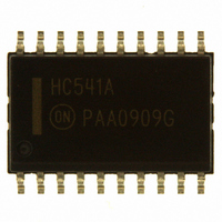
IC BUFF/DVR TRI-ST 8BIT 20SOIC

MC74HC541ADWG

Manufacturer Part Number
MC74HC541ADWG
Description
IC BUFF/DVR TRI-ST 8BIT 20SOIC
Manufacturer
ON Semiconductor
Series
74HCr
Datasheet

Specifications of MC74HC541ADWG

Logic Type
Buffer/Line Driver, Non-Inverting
Number Of Elements
1
Number Of Bits Per Element
8
Current - Output High, Low
7.8mA, 7.8mA
Voltage - Supply
2 V ~ 6 V
Operating Temperature
-55°C ~ 125°C
Mounting Type
Surface Mount
Package / Case
20-SOIC (7.5mm Width)
Logic Family
74HC
Number Of Channels Per Chip
Octal
Polarity
Non-Inverting
Supply Voltage (max)
6 V
Supply Voltage (min)
2 V
Maximum Operating Temperature
125 C
Mounting Style
SMD/SMT
High Level Output Current
- 7.8 mA
Input Bias Current (max)
4 uA
Low Level Output Current
7.8 mA
Maximum Power Dissipation
500 mW
Minimum Operating Temperature
- 55 C
Number Of Lines (input / Output)
3
Output Type
3-State
Propagation Delay Time
80 ns @ 2 V or 30 ns @ 3 V or 18 ns @ 4.5 V or 15 ns @ 6 V
Lead Free Status / RoHS Status
Lead free / RoHS Compliant
Other names
MC74HC541ADWG
MC74HC541ADWGOS

Available stocks

Company
Part Number
Manufacturer
Quantity
Price
Part Number:
MC74HC541ADWG
Manufacturer:
ON
Quantity:
190
MC74HC541A
Octal 3-State Noninverting
Buffer/Line Driver/Line
Receiver
High−Performance Silicon−Gate CMOS
inputs are compatible with Standard CMOS outputs. External pull−up
resistors make them compatible with LSTTL outputs.
receiver designed to be used with 3−state memory address drivers,
clock drivers, and other bus−oriented systems. This device features
inputs and outputs on opposite sides of the package and two ANDed
active−low output enables.
inverting outputs.
Features
*For additional information on our Pb−Free strategy and soldering details, please
© Semiconductor Components Industries, LLC, 2009
March, 2009 − Rev. 6
download the ON Semiconductor Soldering and Mounting Techniques
Reference Manual, SOLDERRM/D.
The MC74HC541A is identical in pinout to the LS541. The device
The HC541A is an octal noninverting buffer/line driver/line
The HC541A is similar in function to the HC540A, which has
Output Drive Capability: 15 LSTTL Loads
Outputs Directly Interface to CMOS, NMOS and TTL
Operating Voltage Range: 2.0 to 6.0 V
Low Input Current: 1 mA
High Noise Immunity Characteristic of CMOS Devices
In Compliance With the JEDEC Standard No. 7A Requirements
Chip Complexity: 134 FETs or 33.5 Equivalent Gates
Pb−Free Packages are Available*
1
20
20
See detailed ordering and shipping information in the package
dimensions section on page 2 of this data sheet.
20
1
20
1
1
1
ORDERING INFORMATION
A
WL, L
YY, Y
WW, W
G
G
(Note: Microdot may be in either location)
http://onsemi.com
DW SUFFIX
CASE 751D
CASE 948E
SOEIAJ−20
DT SUFFIX
TSSOP−20
CASE 738
CASE 967
N SUFFIX
F SUFFIX
SOIC−20
PDIP−20
= Assembly Location
= Wafer Lot
= Year
= Work Week
= Pb−Free Package
= Pb−Free Package
Publication Order Number:
20
20
20
1
20
1
1
1
DIAGRAMS
MC74HC541AN
MC74HC541A/D
MARKING
AWLYYWWG
AWLYYWWG
AWLYWWG
74HC541A
HC541A
ALYWG
541A
HC
G

Related parts for MC74HC541ADWG

MC74HC541ADWG Summary of contents

Page 1

... Chip Complexity: 134 FETs or 33.5 Equivalent Gates • Pb−Free Packages are Available* *For additional information on our Pb−Free strategy and soldering details, please download the ON Semiconductor Soldering and Mounting Techniques Reference Manual, SOLDERRM/D. © Semiconductor Components Industries, LLC, 2009 March, 2009 − Rev. 6 http://onsemi ...

Page 2

... A5 Figure 1. Pinout: 20−Lead Packages (Top View) Data Inputs Output Enables ORDERING INFORMATION Device MC74HC541AN MC74HC541ANG MC74HC541ADW MC74HC541ADWG MC74HC541ADWR2 MC74HC541ADWR2G MC74HC541ADT MC74HC541ADTG MC74HC541ADTR2 MC74HC541ADTR2G MC74HC541AF MC74HC541AFG MC74HC541AFEL MC74HC541AFELG †For information on tape and reel specifications, including part orientation and tape sizes, please refer to our Tape and Reel Packaging Specifications Brochure, BRD8011/D. *This package is inherently Pb− ...

Page 3

... Tested to EIA/JESD22−A114−A. 3. Tested to EIA/JESD22−A115−A. 4. Tested to JESD22−C101−A. 5. Tested to EIA/JESD78. 6. For high frequency or heavy load considerations, see the ON Semiconductor High−Speed CMOS Data Book (DL129/D). RECOMMENDED OPERATING CONDITIONS Symbol Î Î Î Î Î Î Î Î Î Î Î Î Î Î Î Î Î Î Î Î Î Î Î Î Î ...

Page 4

... Maximum Input Capacitance IN C Maximum 3−State Output Capacitance (High Impedance State Output) OUT 9. For propagation delays with loads other than 50 pF, and information on typical parametric values, see the ON Semiconductor High−Speed CMOS Data Book (DL129/D). C Power Dissipation Capacitance (Per Buffer) (Note 10) PD 10. Used to determine the no− ...

Page 5

INPUT A 50% 10% t PLH 90% 50% OUTPUT Y 10% t TLH Figure 3. Switching Waveform OE1 or OE2 50 PZL PLZ OUTPUT Y 50% t PZH OUTPUT Y 50% Figure 4. Switching Waveform ...

Page 6

INPUTS A1, A2, A3, A4, A5, A6, A7, A8 (PINS Data input pins. Data on these pins appear in non−inverted form on the corresponding Y outputs, when the outputs are enabled. CONTROLS ...

Page 7

SEATING PLANE 20X 0. 18X PACKAGE DIMENSIONS PDIP−20 N SUFFIX PLASTIC DIP PACKAGE CASE 738−03 ISSUE ...

Page 8

K 20X REF 0.10 (0.004) 0.15 (0.006 L PIN 1 IDENT 1 0.15 (0.006 −V− 0.100 (0.004) −T− SEATING PLANE 16X 0.36 PACKAGE DIMENSIONS TSSOP−20 DT SUFFIX ...

Page 9

... Opportunity/Affirmative Action Employer. This literature is subject to all applicable copyright laws and is not for resale in any manner. PUBLICATION ORDERING INFORMATION LITERATURE FULFILLMENT: Literature Distribution Center for ON Semiconductor P.O. Box 5163, Denver, Colorado 80217 USA Phone: 303−675−2175 or 800−344−3860 Toll Free USA/Canada Fax: 303− ...

Related keywords